 hesam.moshiri
DC to DC buck converters is a famous topology in the electronic and a widely used circuit in electronic devices. A buck converter steps down the input voltage while it increases the output current. In this article/video, I have discussed a DC to DC buck converter that can be used effectively as a switching power supply. The output voltage and current are adjustable: 1.25V to 30V and 10mA to 6A (continuous). The power supply supports the constant voltage (CV) and constant current (CC) features. Two LEDs demonstrate the CV and CC status. The circuit is compact and both sides of the PCB have been used to mount the components.
To design the schematic and PCB, I used Altium Designer 21, also the SamacSys component libraries (Altium plugin) to install the missing schematic symbols/PCB footprints. To get high-quality fabricated PCB boards, I sent the Gerbers to PCBWay.
To test the circuit, I used the power analysis feature of the Siglent SDS2102X Plus oscilloscope (or SDS1104X-E), Siglent SDL1020X-E DC Load, and Siglent SDM3045X multimeter. Isn’t cool, so let’s get started!
Specifications
- Input Voltage: 8V to 35VDC
- Output Voltage: 1.25V to 32VDC
- Output Current (continuous): 10mA to 6A
- Output Current (short period): 7A to 8A
- Output Noise (no load): 6mVrms (9mVp-p)
- Output Noise (6A load): 7mVrms (85mVp-p)
- Output Noise (6A load, 16P-average): 50mVp-p
- Efficiency: up to 96>#/li###
A. Circuit Analysis
Figure 1 shows the schematic diagram of the switching power supply (DC to DC buck converter). The schematic diagram contains 3 main parts: the buck converter, feedback loop, and opamp regulator.

Figure 1, schematic diagram of the adjustable switching power supply
PSI is the XL4016 controller chip [1] and the main component of the buck converter. D2 is the MBR20100 Schottky diode [2] and L2 is a 47uH-10A inductor that are other essential components of the buck converter circuit. C3..C9 are used to reduce the input/output noises.
R2 is a 20K multiturn potentiometer (trimmer) that provides a feedback path to the controller chip to adjust the output voltage. C1 is used to reduce the noise on the feedback path. R1 is just a 0R resistor that is used as a jumper on the PCB board. R4 is the shunt resistor that is made of two 0.1R-5W resistors. These two resistors are connected in parallel to make a single 0.05R-10W resistor.
IC2 is the TS4264 linear regulator chip [3] that provides a stable +5V supply rail. C15 is used to reduce the output noise of the regulator.
IC1 is the MCP6002 opamp [4] that is used to amplify the small shunt resistor voltage to provoke the feedback pin of the PS1. D1 provides a feedback path to the PS1. The MCP6002 chip provides two opamps. The first opamp is configured as a non-inverting amplifier and the second opamp is configured as a comparator to feed D3 and D4 LEDs (CC, CC). R5, C11..C13 create a low pass RC filter to reduce the supply noise to IC1. R9 and C14 also build a low pass RC filter to remove the shunt noises. C10 is also used to reduce the amplifier noise.
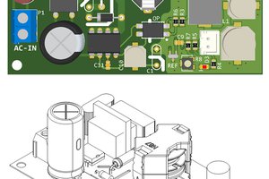
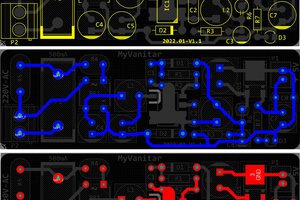
B. PCB Layout
Figure 2 shows the PCB layout of the variable switching power supply board. It is a two layers PCB board and a mixture of SMD and through-hole components have been used to make it as compact as possible.

Figure 2, PCB layout of the adjustable switching power supply
I used the Altium Designer software [5] to design the schematic and PCB. I did not have the schematic symbols, PCB footprints, and 3D models of several components in this project. So instead of wasting my time in designing the component libraries from scratch and increase the risk of errors and mismatches, I used the free and IPC-rated SamacSys component libraries and imported them right into the Altium PCB project using the SamacSys Altium plugin [6]. SamacSys provides plugins for the majority of electronic designing CAD software [7], not just for the Altium Designer. Figure 3 shows the supported electronic designing CAD software.

Figure 3, SamacSys Supported electronic designing...
Read more »

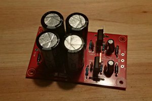
Many of us actually build power supplies for internal use but not always showing them. I made a couple dc-dc buck converters based on L4978.