 Colin Maykish
Component Boards
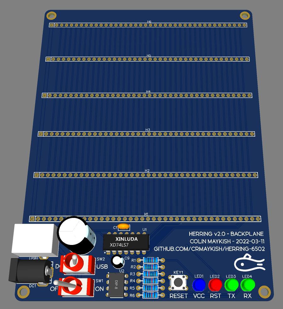
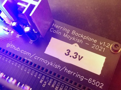
Backplane
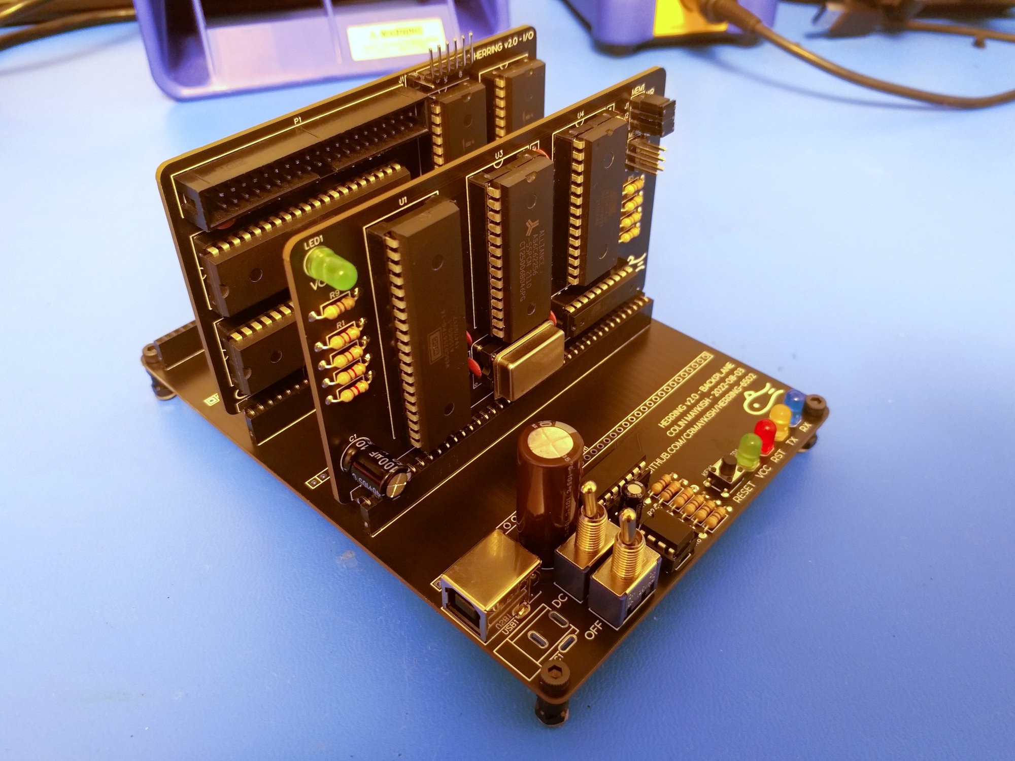
Herring is designed as a passive backplane system. The backplane PCB provides DC input, a 5v regulator, a reset button and the system bus. Everything else is done on the individual boards.
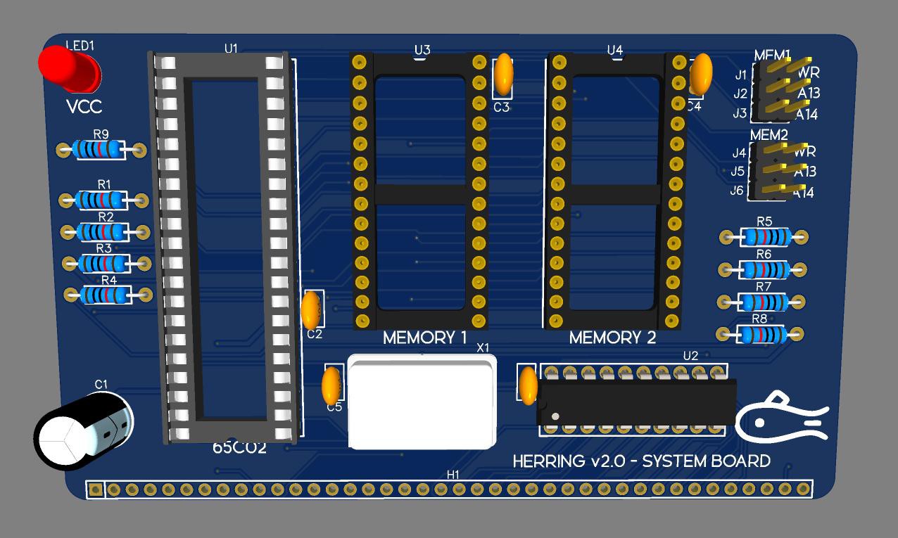
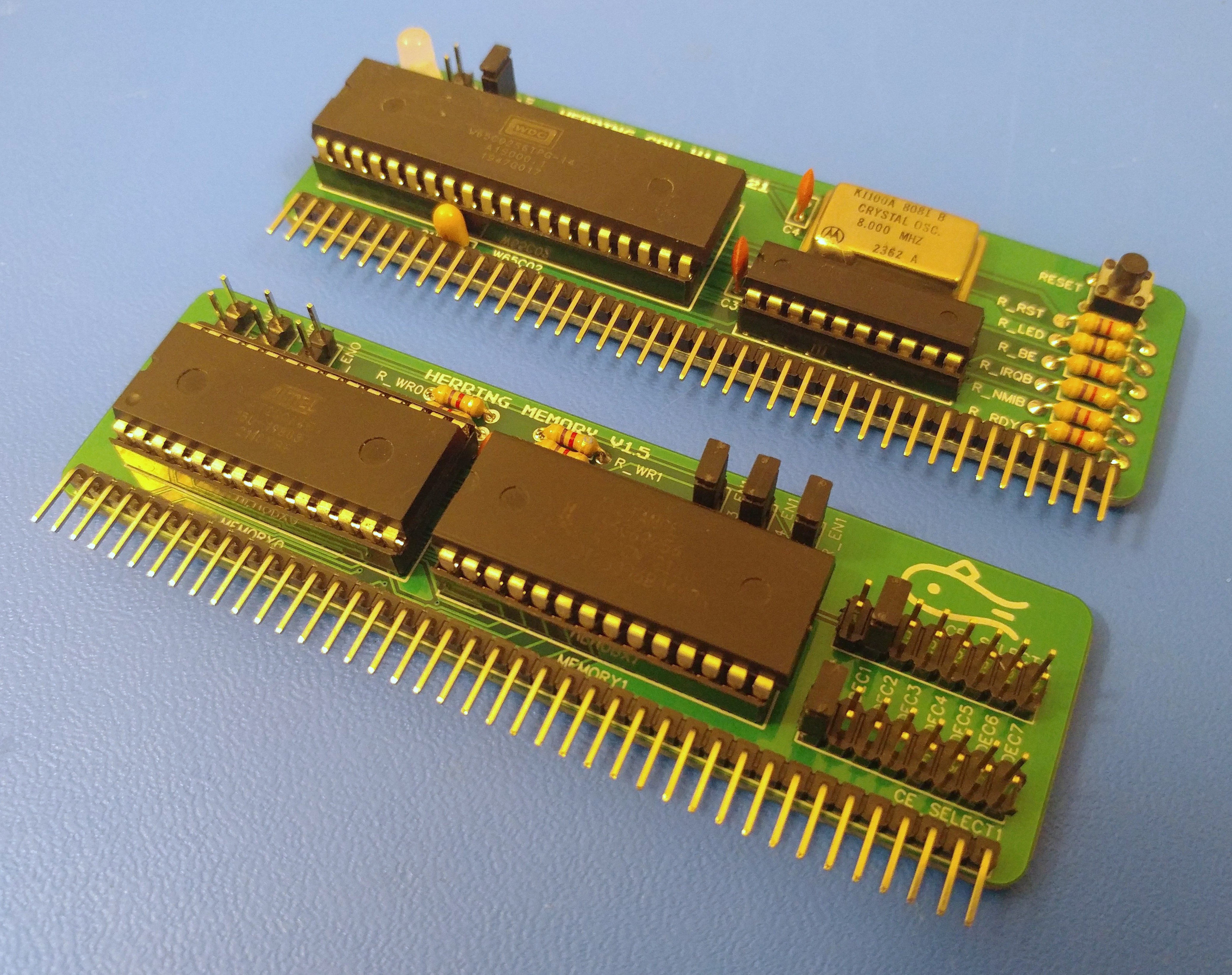
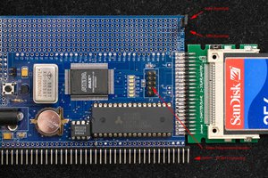
CPU Board
Fits a 6502 CPU. Connects address and data buses as well as most of the CPU control lines directly to the system bus.
This board also provides a system clock in the form of an oscillator and address decoding / glue logic with a ATF16V8B GAL chip. The GAL takes in address and control lines from the CPU and outputs eight "decoder" lines that can be used as chip-select pins for the various peripheral boards.
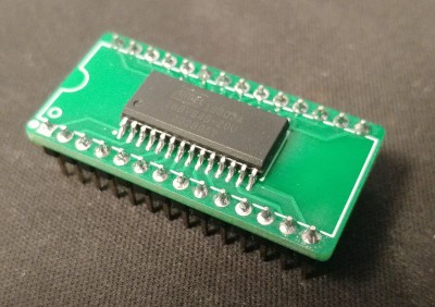
Memory Board
Each memory board holds two 8KB or 32KB ROM or RAM chips. The size and type of each chip is configurable with onboard jumpers. Each memory chip can have its chip-select pin mapped to directly to A15 or one of the DEC lines to allow for a flexible memory map.
The base system is designed with a single 8KB ROM and 32KB RAM board installed. Technically, multiple memory boards can be installed in parallel to add additional ROM and RAM, but there is currently no memory banking, so one memory board seems sufficient for most applications.
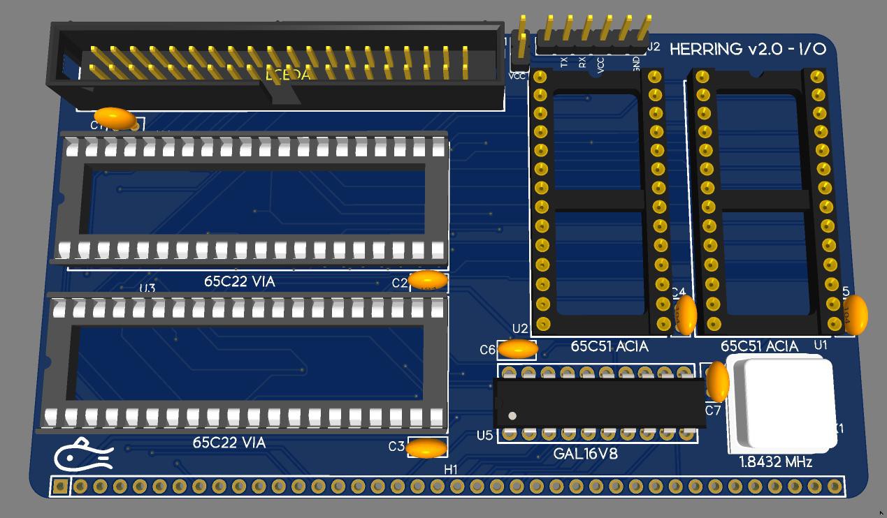
GPIO Board
A 6522 VIA chip is used to provide 16 GPIO lines. These I/O pins are exposed on a 2x10 pin header, allowing jumper wire or ribbon cable connections to peripherals. Herring also makes use of the VIA for its timers.
Serial Board
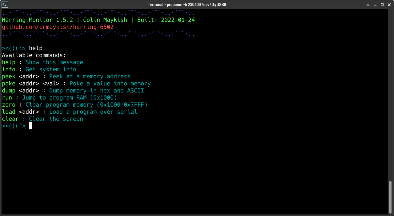
A 6551 ACIA creates a simple UART for the system. This serial port can run at up to 230400 baud. An onboard 1.8432 MHz or 3.6864 MHz crystal provides the ACIA with a clock for its internal baudrate generation.
Multiple serial boards can also be installed in parallel. I'm currently using one for the console and one for experimentation with other serial peripherals. Each board can be assigned to a unique memory address range using the decoder GAL.
System Bus Pin Description
The system bus has changed slightly as new iterations of Herring have been built, but this is the up-to-date pinout for v1.5.
The system bus consists of a single 40 pin header. The pins are in order as follows:
1. VCC - 5v regulated input
2. GND - ground connection
3-10. Data pin 0 through data pin 7
11-26. Address pin 0 through address pin 15
27. /RES - system reset pin
28. CLK - system clock (oscillator is connected directly to this line)
29. RW - read/write pin on the 6502
30. /IRQ - interrupt request
31-38. /DEC0 - /DEC7, used for peripheral chip-select, driven by the GAL on the CPU board
39. BE - Bus enable pin on the 6502, pull low to allow another bus master (currently this is not a feature I've implemented)
40. GND - ground connection

 Tobias Rathje
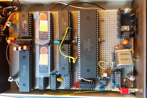
 Plasmode
 Dean Netherton
Great Idea! It looks like a 6502 version of RC2014. Do you plan to publish/upload schematics for the backplane, processor, memory, etc? I would like to build a system.