I finally found some motivation to start tracing the missing boards (EAGLE files are in the "files" section of the projects).
The CPU board
I started with the CPU board:
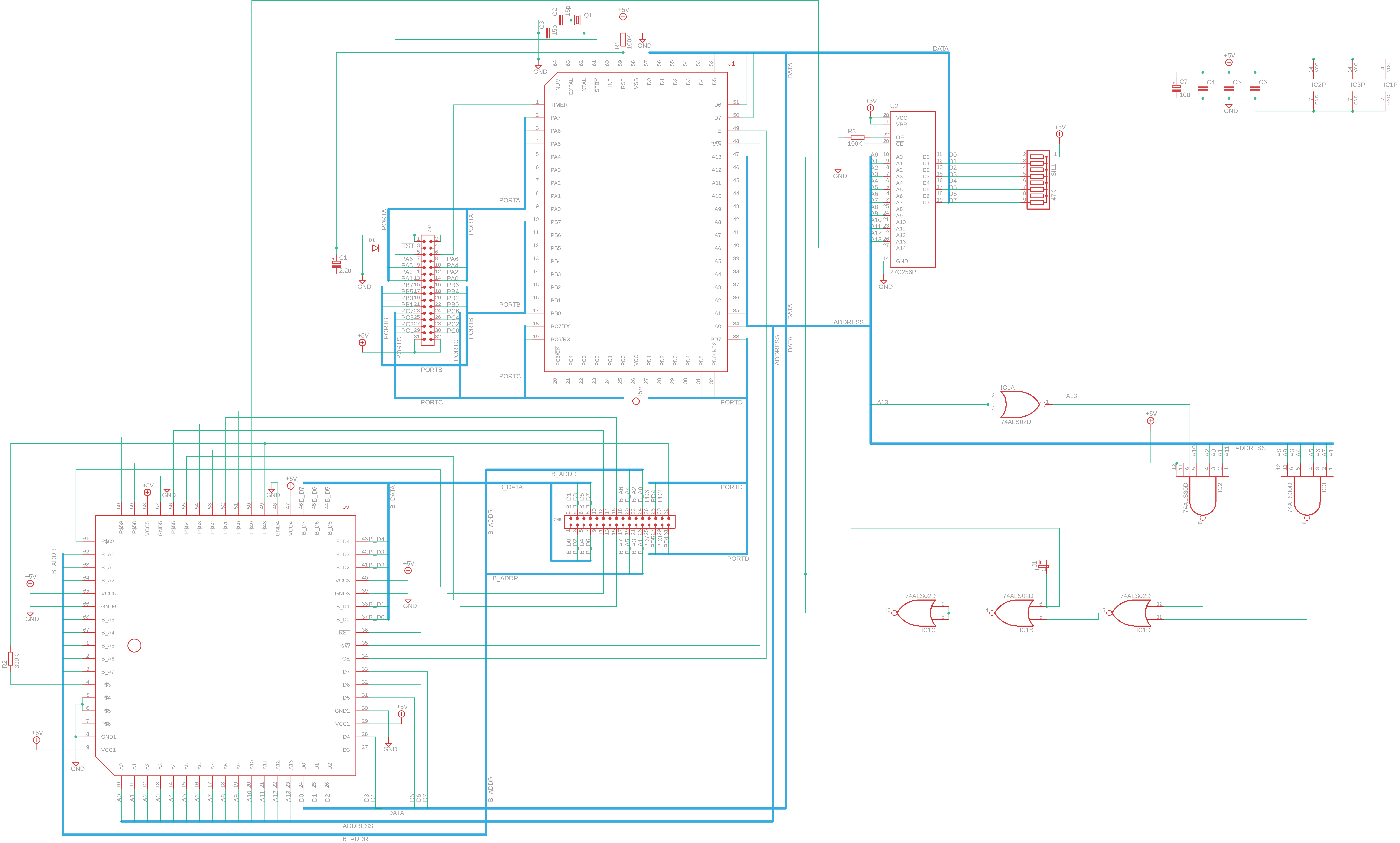
A few observations, in random order:
- Connector CNA has MCU I/O ports A, B and C plus interrupt and standby signals
- The "mistery" SCL1054-V4 (U3) chip directly hooks up to the MCU's data and address buses
- CNB has input port PORTD and a bunch of signals from U3
The first thing that caught my attention is that the MCU's address and data buses are not exposed to the main board, as I would've thought based on the number of pins on the connectors. How are the external RAM and the config ROM connected to the system then? I was a bit puzzled, but I figured it'd be more clear once I looked at the other boards.
I then started looking into the address decode logic, since I needed to know where the ROM was mapped in the memory space to decompile the code. Looking at the Hitachi manual, here's the basic memory map:
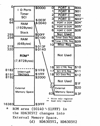
So, the available range for ROM and/or other memory mapped devices is 0x0140-0x3FFF (plus a tiny slice from 0x0020 to 0x003F). Here's where things get bizarre again:
First of all, U3 can disable the ROM through IC1B (or, on boards where the three 74xx series chips are missing and J1 is installed, can control the ROM directly). This is somewhat strange but not totally unexpected, so I moved on. Then I found another problem: if you follow the schematics, you'll see that the chip enable output from the CPU (which is bizarrely active HIGH) is totally ignored by the ROM selection logic and only routed to U3. I checked the Hitachi manual and in the section about connecting an external ROM (PDF page 227, section 3.1.1) it shows a schematic which completely ignores the !CE and !OE pins, so either the internal data bus buffer goes HI-Z automatically when accessing internal RAM/registers (which would make sense, since the diagrams show that there's indeed a buffer), or they put some extra decode logic inside U3 to deselect the ROM when needed.
What really confused me (and I still can't explain) is that the only address where the onboard selection logic (IC1, IC2 and IC3) explicitly deselects the ROM is 0x1FFF; if you check the Hitachi manuals again, you'll see that the reset interrupt vector is stored in ROM at 0x1FFE-0x1FFF (it's a 16 bit pointer to the address of the first instruction to execute, stored big endian), so I really don't understand why you wouldn't want the ROM to be selected while reading that.
The RAM board
With these discoveries, I moved on the RAM board:
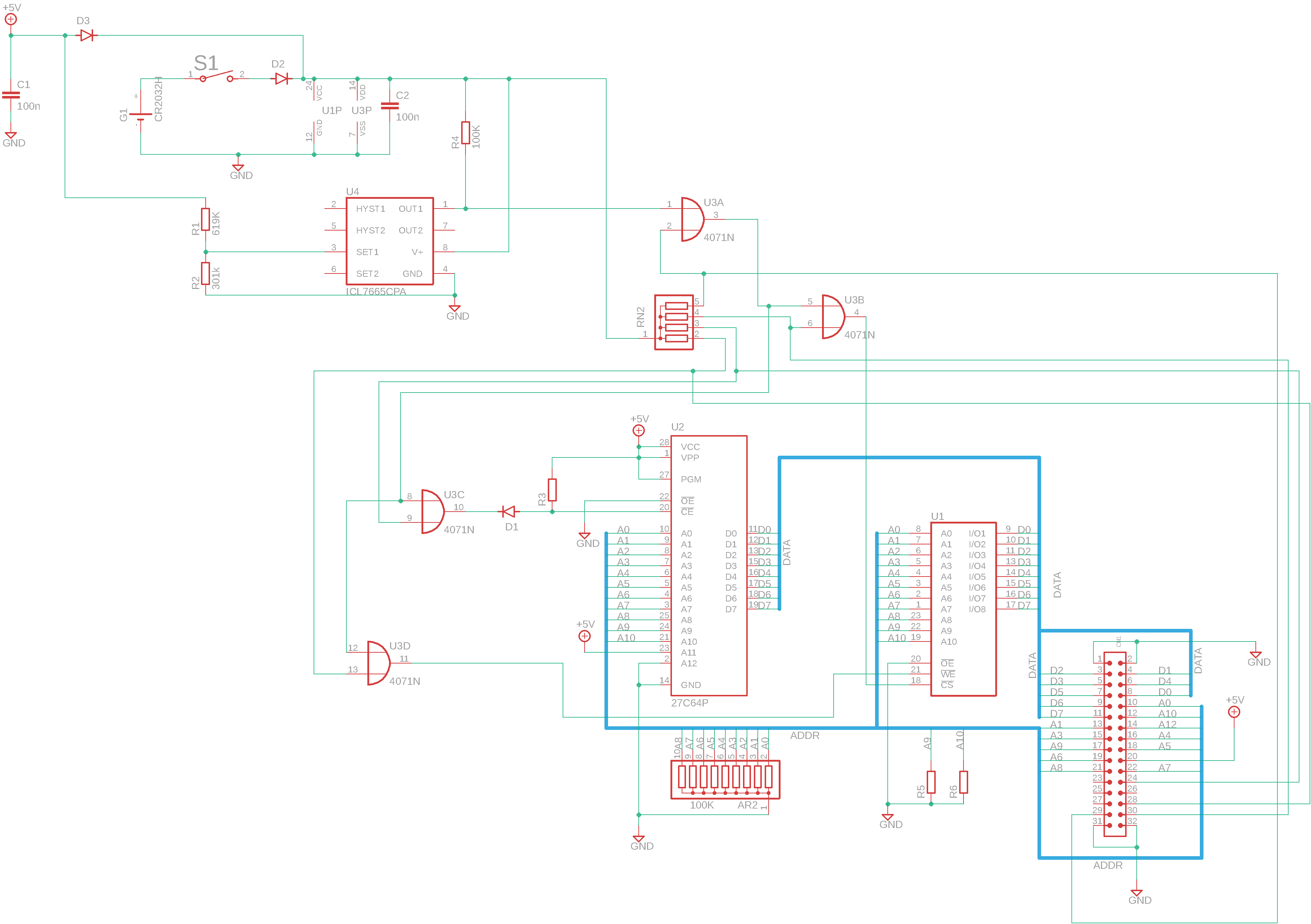
This section here is pretty straightforward. ROM and RAM share the same address and data buses, both of which are exposed to the main board through the only connector present (only address lines A1 to A8 seem to actually be in use, but A9 to A12 are still present on the connector). There's some 40xx series logic that selects the two memory chips (interestingly, they're toggling the !CE line and not the !OE line to select the chips, as they do on the CPU board; this works, but I've usually seen it done the other way round), with the inputs connected to some signals I haven't yet identified (perhaps some kind of bus, since there's a resistor array connected to the four lines?). A small lithium cell is connected to the RAM to retain the data even without power, and an Intersil ICL7665 is used to alert the system when the battery runs low.
This still does not solve the problem of "what is this memory hooked up to?", though, so I started looking at the main board
The main board
I'm still working on the main board (there's a lot more stuff going on there), but I've traced enough of it to find out where the RAM board connects to; if you've looked at the CPU board schematics carefully, you probably already found the answer: it hooks up to the SCL1054-V4 chip, through a second set of address and data buses. This, combined with what I already knew from tracing the other board, allowed me to figure out what most of the pin of the chip are.
Continuing with the code disassembly
I chose to ignore for now the fact that low byte of the reset vector in ROM is ignored and just disassemble the ROM as is.
Having determined the memory map, I can now import the ROM image in Ghidra with the right settings:
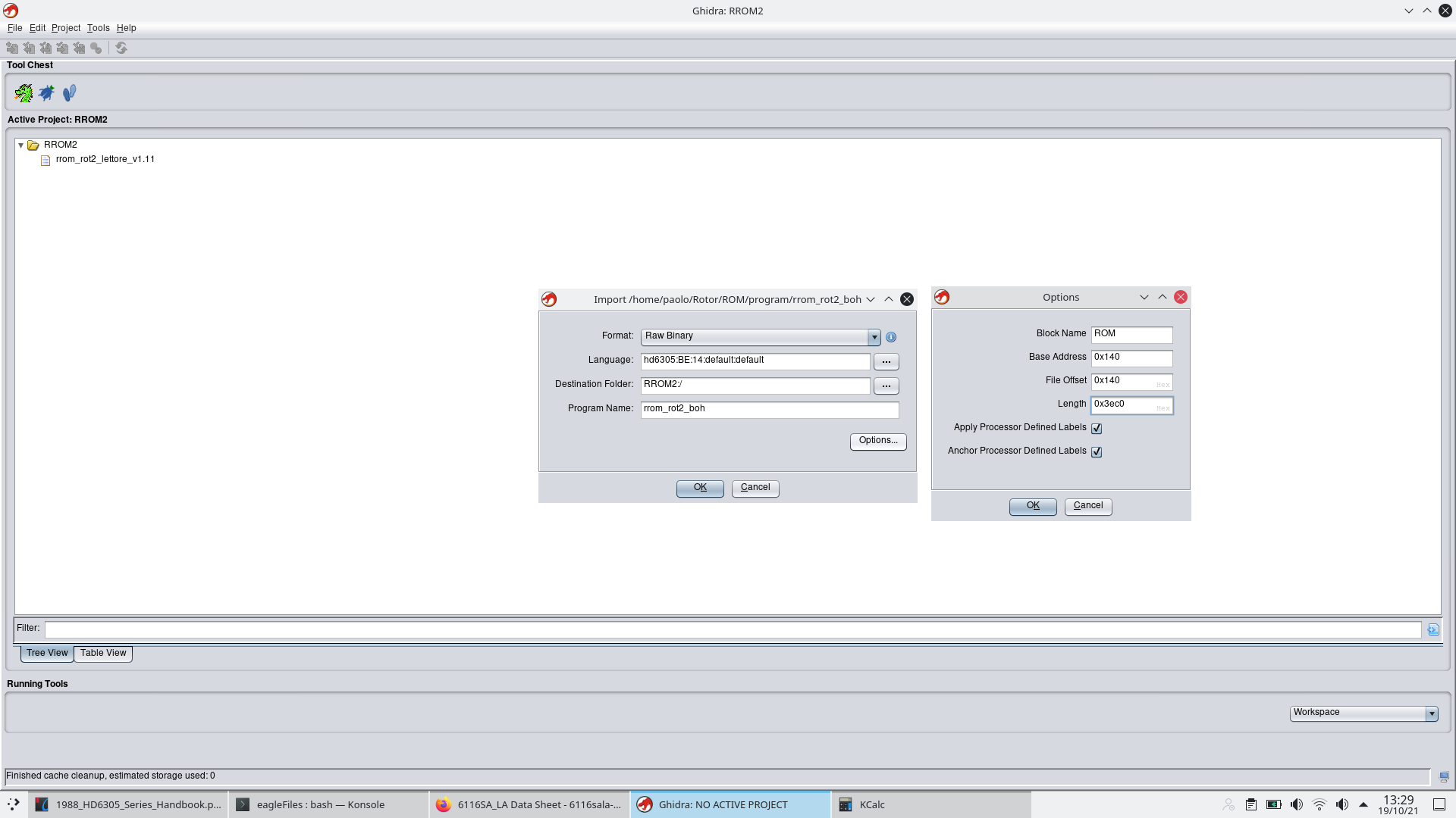
(file offset 0x0140, mapped in processor address space starting from 0x0140)
I then scrolled down to 0x1FF6 to look at the vectors:
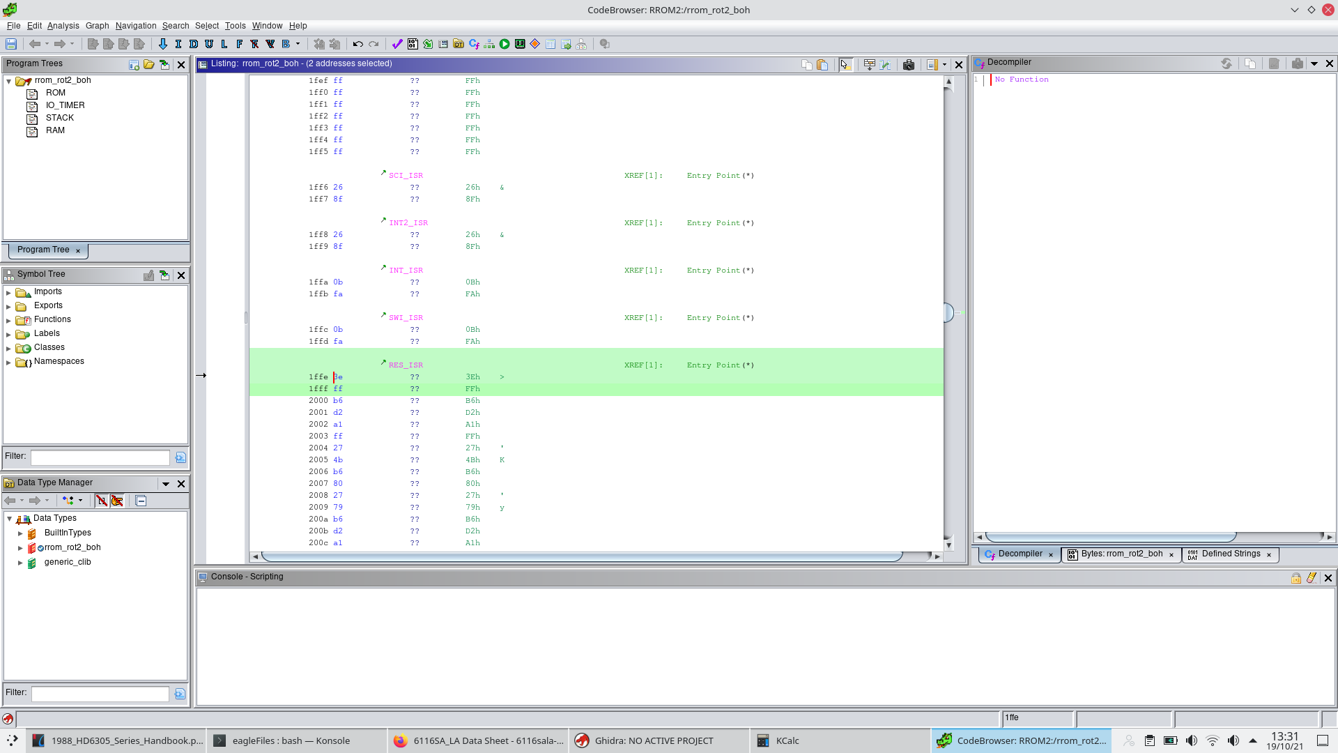
The values here seem reasonable (they're both address in the external memory range, and the fact that some of them match makes them seem even more plausible).
I then jumped at the address specified for the reset vector (0x3EFF):
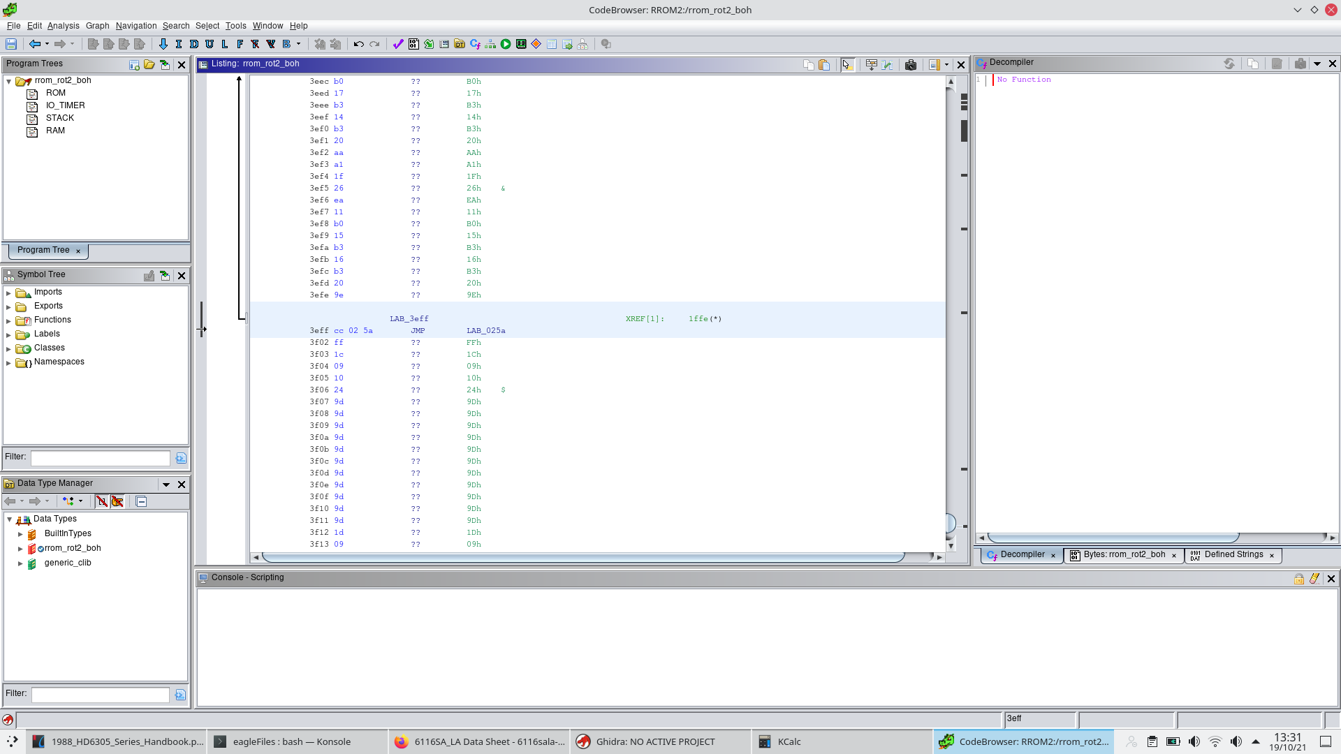
As you can see from the picture, it's a jump instruction. I followed the jump, and...
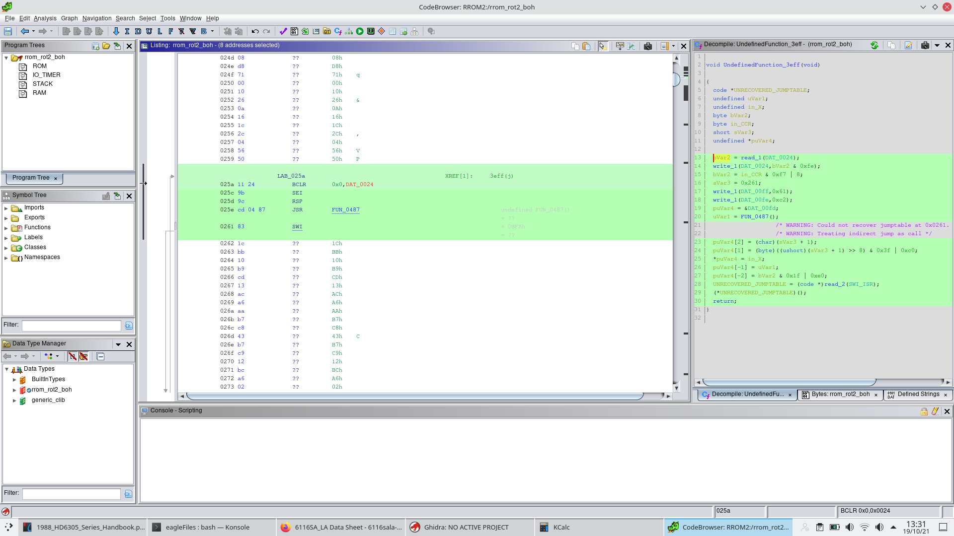
Eureka! The code clears some location in memory, enables interrupts, resets the stack pointer and jumps to a function; this looks to me like it's the code that initializes the whole systems.
I then looked at the subroutine it calls. This is where I realized I had an error in my Ghidra processor module: it wasn't calculating the return addresses correctly and getting confused; long story short, I was popping them from the stack in the wrong order (I forgot to increment the Stack Pointer BEFORE trying to retrieve PCH and PCL) and I was manipulating the program counter register directly instead of using the appropriate Sleigh instruction "return". I uploaded a fixed version of the processor module in the files.
After the appropriate corrections, I got this:
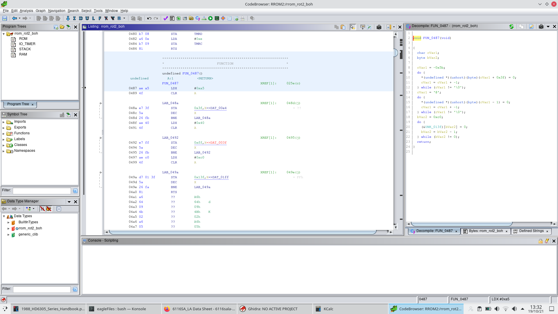
Again, it's clearing some memory, so it's likely initialization code. I didn't get much farther than this for now. but at least this tells me that my processor module is working AND I got a valid ROM dump.
New parts!
This is the part I'm most excited about! As I was looking on local auction sites, I found a very strange object listed a bunch of keywords like "SIP Rotor", "G + M", "Public phone" and so on; Upon looking at the picture, I found out it was a brand new spare card reader module! Basically, it's the whole card reader without the metal enclosure. It was cheap enough (50€) that I could justify buying it! i've not received it yet, but I already made some interesting discoveries (spoiler alert!): apparently, the card reader is smarter than I thought, as it is equipped with its own microcontroller (the same Hitachi chip) and its own ROM. It probably talks to the main chip via serial (I've found some serial port init code while skimming the disassembly), so maybe I can even interface it to a modern microcontroller and make it work again.
Stay tuned for more updates!
Discussions
Become a Hackaday.io Member
Create an account to leave a comment. Already have an account? Log In.