 Keith
KeithIC15, TPAL, Timing PAL
We can see that pins 19,18,17 are a simple clocked counter. Other signals control DRAM, and other designs might provide a starting model. The RAM is interleaved VDU/CPU access, so the DRAM signals may only begin just after the VDU phase has finished.

I suspect that this forms a state machine with 8 states per memory cycle, and generates a fixed sequence of DRAM access signals from those states. Which makes sense, because the 6845 does not do that. I also suspect it generates the same sequence for CPU access, but simply making the CPU wait until it is complete.
Scoping the signals would give a good idea of the DRAM signals to be created.
Alternatively, you might be able to tell the PAL it is doing video cycles, and then record the state of the output pins as it is clocked. Pins 17, 18 and 19 are going to cycle through states 0 to 7, and the DRAM control signals should change at the same states throughout an 8-state memory cycle.
It is worth noting that the microprocessors of the 1980s all ran at pretty much the same memory cycle rate. A 1 MHz 6502 had 1 clock per memory cycle, a 4 MHz Z80 had 3 or 4 clocks per memory cycle, and an 8 MHz 68000 had 8 clocks per memory cycle. All of these would have around the same 1 MHz memory cycle rate.
If you get the DRAM signals wrong, the computer will crash straight away, so I doubt it would have time to do any damage to the 1616. You could make a small gadget that turns off the 1616 if does not run some code that disables the gadget in time. This would prevent the 1616 running for any significant length of time with a non-valid DRAM interface.
The 68000 memory read cycle
... looks like this:
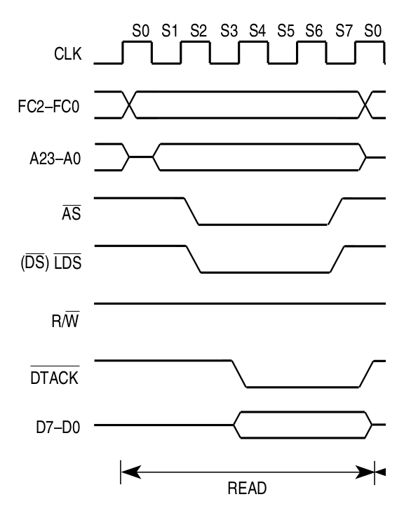
So I would expect a /RAS signal to be similar to /AS, with /CASU and /CASL to resemble /UDS and /LDS respectively.
The DRAM control signals will be a function of the signals on pins 17 to 19.
To find the timing, one would have to tell the PAL it is in video cycles (using DISPEN?) and then toggle the clock (pin1) and record the state of the outputs as they cycle through eight states.
This can be done at human speed, just by applying a debounced pulse on pin 1.
Until that gets done, I will look for existing 68000 DRAM interfaces. This is hard to find, as it is not the sort of thing people tackled unless they were a big company. However, I did find a book that covered the subject in great detail:
68000 hardware, software, and interfacing by Allan Clements.
After much text about DRAM in general, it presents a 68000 to DRAM timing diagram on page 390:
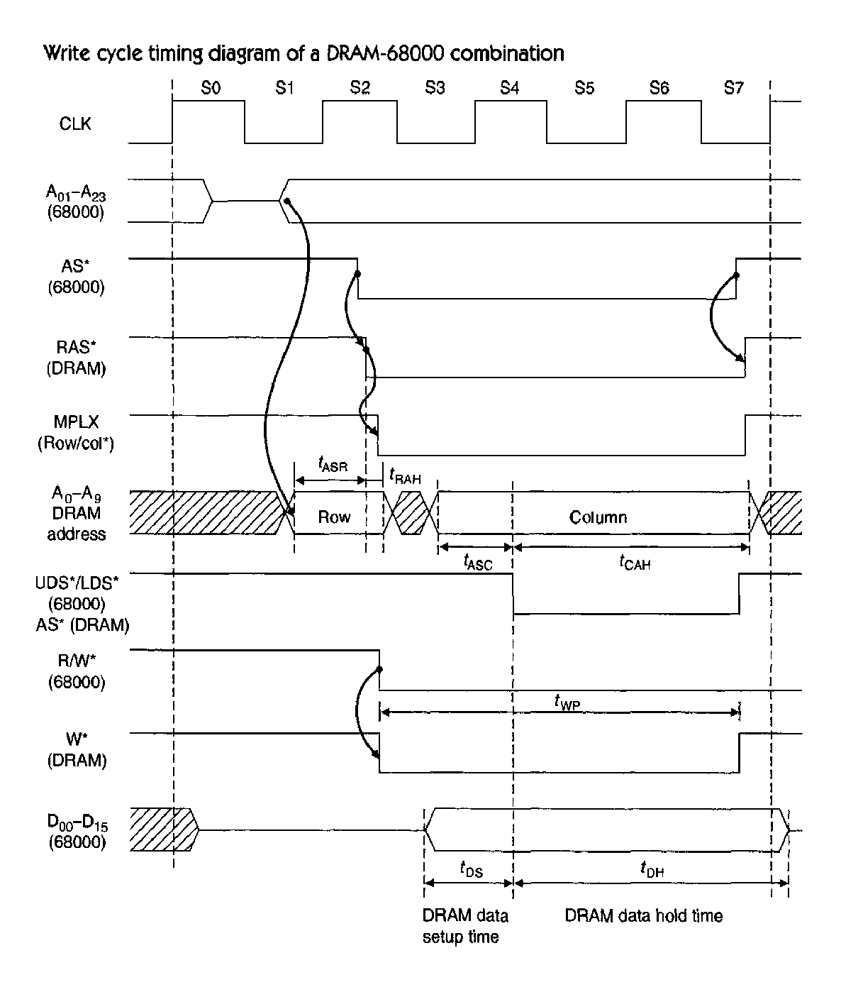
This provides a good starting point where there is only one DRAM access per CPU cycle. /AS is effectively /RAS and /DS is effectively /CAS.
For interleaved video/CPU access, the CPU DRAM access must be crammed into the second half (S4-7) and the video access crammed into the first half (S0-3).
Example timings are hard to find. This sort of thing goes on in the 1616, the Apple Mac, the Atari ST, the Commodore Amiga, The Sinclair QL.... but manufacturers were not keen on disclosing such details.
I eventually found some timings from some files salvaged from Atari after they went bust. Here is the timing of one of their chips:
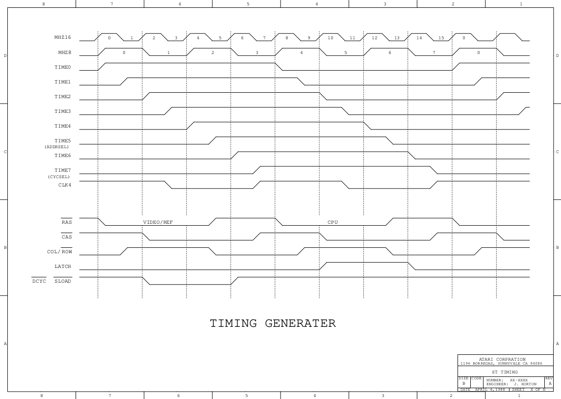
For the 1616, the signals "MHZ16" and "MHZ8" would be the 15 and 7.5 MHz clocks respectively.
The MHZ8 signal has the numbers 0 to 7, representing the 68000 CPU states S0 to S7.
The Atari ASIC derives timings by shifting a 2 MHz square wave through an 8-bit shift register at 32 MHz. This makes it easy to decode timings with very little logic. For instance:
/SLOAD =  TIME2 * /TIME6 ; /* a NAND and NOT gate for single pulse */
LATCH  = /TIME2 *  TIME6 ;
/RAS   =  TIME0 * /TIME5 + /TIME0 * TIME5 ; /* a XOR gate for double pulses */
COL    =  TIME1 * /TIME5 + /TIME1 * TIME5 ;
/CAS   =  TIME2 * /TIME7 + /TIME2 * TIME7 ;
CLK4   = /TIME3 * /TIME7 +  TIME3 * TIME7 ;
The 1616 TPAL derives timings by using its 30 and 15 MHz inputs and a 3-bit synchronous counter. That gives 5-bit resolution, same as the Atari. Other logic generates the ROW/COL signal (just delayed /RAS ?).
So it is looking very possible to generate Atari timings in a 1616 GAL chip. This can then run in parallel with an original 1616 chip and the signals compared. The logic can then be tweaked until they are identical.
I have made a spreadsheet to confirm the logic above.
The actual circuit and timings are shown here: Atari_timing_from_ASIC_ST4081S_page_7,8,48,49.pdf
The shift register is simple and economical of silicon chip area, but the 1616 timing PAL16R8 has to use three pins for a 3-bit counter in order to have five pins left for control outputs. If it is a simple binary counter, multiple bits may change on the clock edge. So any logic derived fed by them must be clocked to avoid glitches, but the 16R8 can provide that.
The PAL does not have to generate the row/column select signal, as this is simply /RAS delayed by one clock cycle in U50b.
I've just found a timing diagram for the Apple Lisa:

The RAS and CAS signals have very similar timings. High for 3 dot clocks and low for 5. The CAS signal is RAS delayed by 2 dot clocks.
Looking at the Texas 4164 datasheet page 9, and the 200ns access time device, the minimum times for RAS high and low are 120 and 200 ns respectively, which is in the ratio of 3 to 5. That device has a read cycle time of 330 ns, which is fast enough for 500ns of a 2 MHz cycle rate (twice the 1 MHz cycle rate of a 68000 clocked at 8 MHz).
For a 16 MHz 68000, the cycle times are halved to 250ns. The 150ns 4164 has a cycle time of 260 ns which is 10ns longer but in practice devices are rated conservatively. They are not rated at their extreme limits. For the 150 and 120 ns devices, the RAS high:low times are 100:150 and 80:120 respectively, both having a ratio of 2:3.
Dividing 8 dot clocks in the ratio 2:3 give 3.2 to 4.8. So 3:5 is still the nearest integer ratio. For a 16 MHz CPU clock, and 250 ns memory cycle, RAS high:low would be 93.75 : 156.25 ns, which a 150 ns part might manage and a 120ns part would be within spec.
I conclude that the RAS and CAS timing for the Atari and Apple Mac should suit the Applix 1616.
Discussions
Become a Hackaday.io Member
Create an account to leave a comment. Already have an account? Log In.