 Keith
KeithU24 ("SPAL") - the expansion bus interface logic
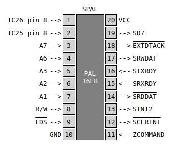
Pins 1 and 2 go low at the I/O space (A23 to A8 are high). A7-A1, R/W, and /LDS are basic 68000 signals.
The manual states that the memory map looks like this:
$FFFFFC1 R/W    ZDATA     Read:  Data from Z80.
                          Write: Data to Z80.
$FFFFC3 Read   SCLRINT    Clear 1616 interrupt.
$FFFFC3 Write  SINTZ      Interrupt Z80.
$FFFFC9 Read   SRXRDY     Bit 7 set if receive latch full.
$FFFFCB Read   STXRDY     Bit 7 set if transmit latch empty.
$FFFFCD Read   ZCOMMAND   Bit 7 set if contents of the receive latch
                          is a command.
$FFFFD1 Write  SCOMMAND   Write data to the data latch,
                          set SCOMMAND bit.
The PAL multiplexes SRXRDY and STXRDY onto SD7.
Basically the two processors communicate through two 8-bit latches.
This all looks pretty simple to implement.
The binary behaviour data seems wrong, because pin 18 is listed as an input when it should be an output.
So I just had a quick go at deducing the logic by reading the manual and the circuit.
Discussions
Become a Hackaday.io Member
Create an account to leave a comment. Already have an account? Log In.