 Dave Collins
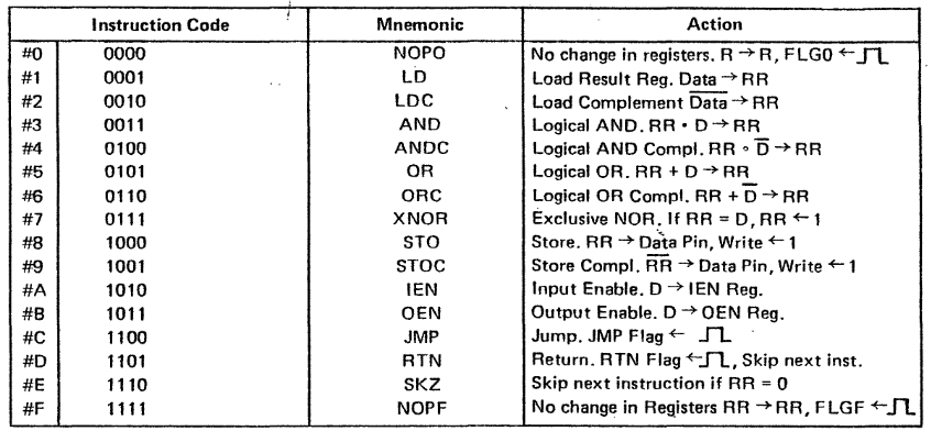
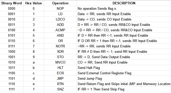
This is my CPU project, that was born out of trying to build 1 - bit combination logic ALU's from op-amps. In doing the research for that project I determined that much of the MC14500 is a relatively simple (still a large number of transistors) finite state machine. I decided to see if I could build a relatively fast state machine out of EEPROMS and D-Latches.
This project is very similar, and very much inspired by the UE14500 Vacuum tube computer Project.
My project goals are:
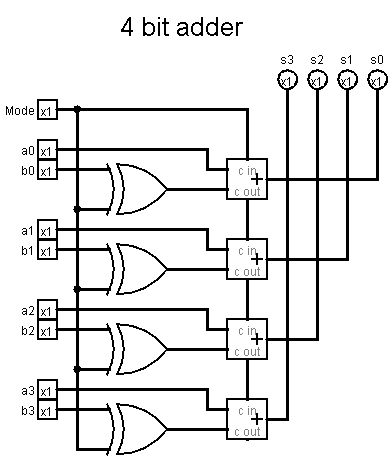
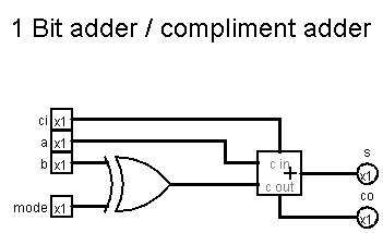
- Design the logic for the state machine I want to build (this is in it's first draft)
- Design / build / adapt? a work flow for simply making changes by either building or modifying existing tools for making binaries so that development is less cumbersome.
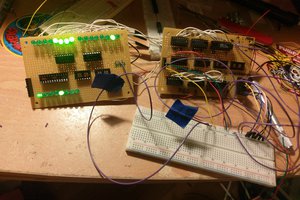
- Build a prototype on a breadboard to demonstrate a proof of concept using an 8-bit addressable d-latchs and some switches that can be used to compare 2 8 bit numbers and update a 8-bit display latch.
- Build a prototype, that is Turing-Complete with expanded functionality for moving 8bit data, jump / return and write a machine language monitor.
 Boxerbomb
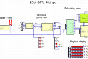
 Pavel
Pavel
 Dave's Dev Lab
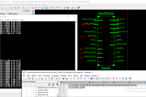
 zpekic