Close
0%
0%

Custom circuit testing using Intel HEX files

Download / upload memory contents into computer motherboards or other devices for test or debugging (using 3 micro-coded controllers)

Public Chat
Similar projects worth following
FPGAs wired to the outside word can be a powerful and flexible tool for all sorts of applications, among them testing PCBs with any sort of memory chips. As long as one can get hold of the system bus, memory contents can be extracted and uploaded, inspected on the host computer etc. The approach will work even if the target system is in various levels of "dead".

A still popular format for capturing memory content is Intel HEX files. Typically, processing these files requires a microprocessor / microcontroller (physical or soft-core on FPGA). This design does not use any of that, instead two custom micro-coded controllers take that work, one converts HEX character stream to memory write sequences, and the other one the opposite. For fun, a 3rd custom micro-coded controller is thrown in, which acts like a simple "VT-52" type device (to VGA)

In this project, I use it to test a 8085-based single board computer, for a last sanity check before populating it with CPU

This project builds upon my previous Intel HEX project which I developed to:
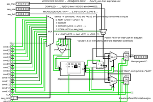

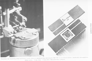
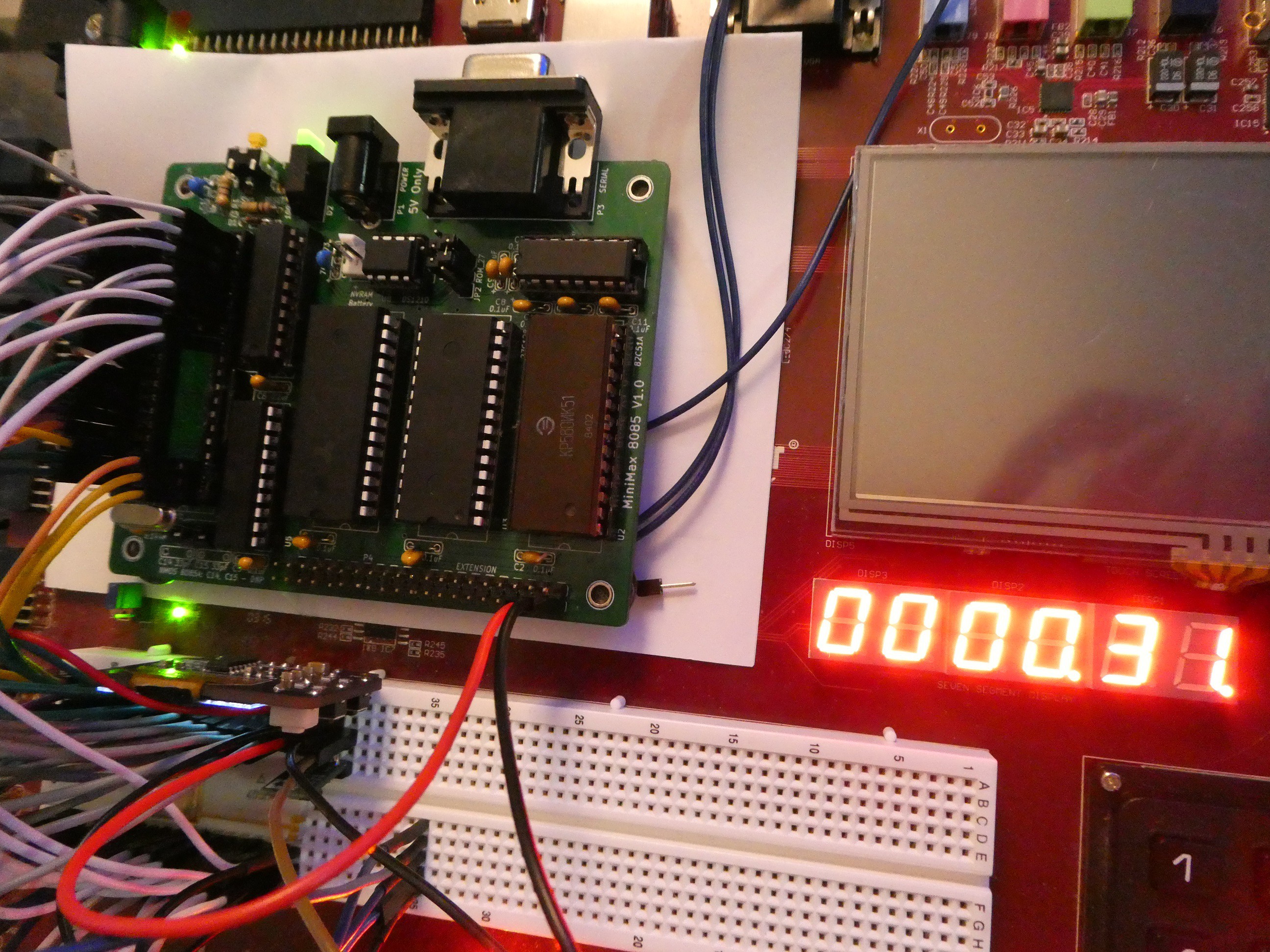
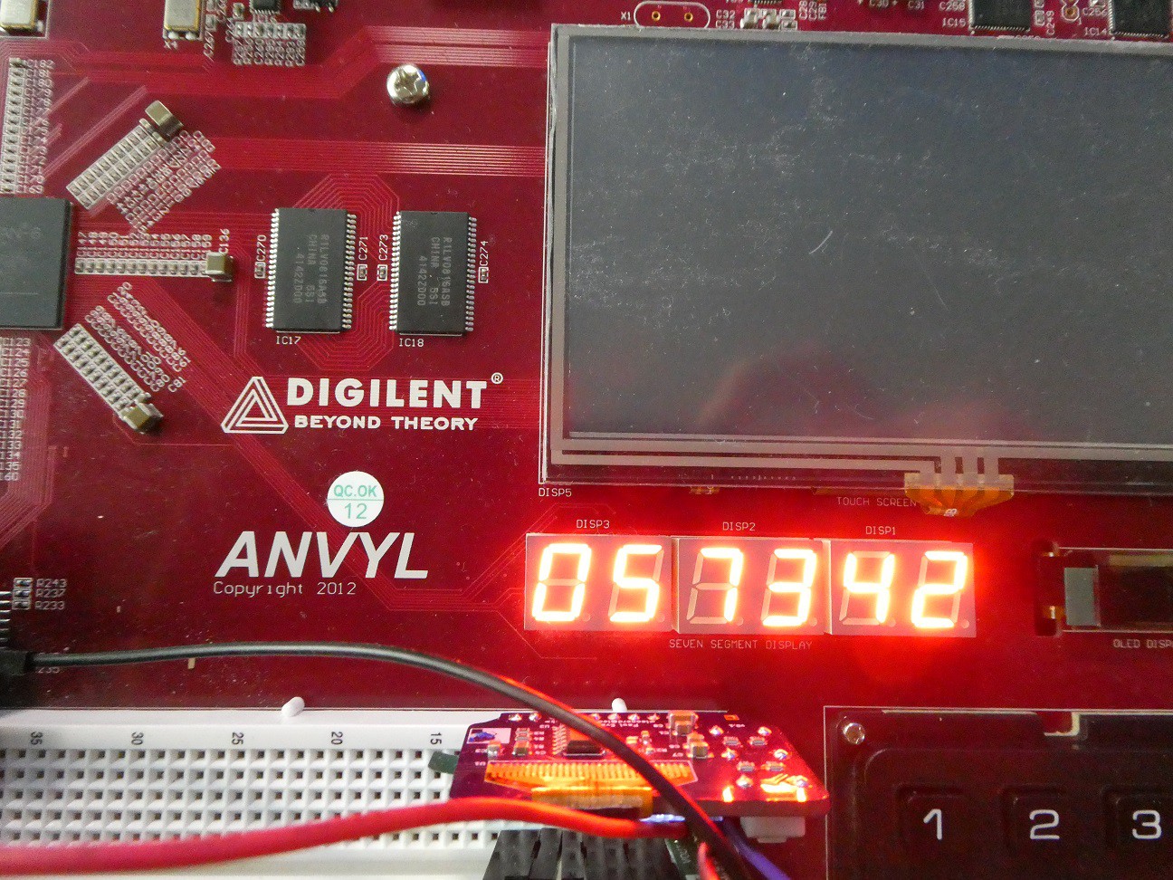
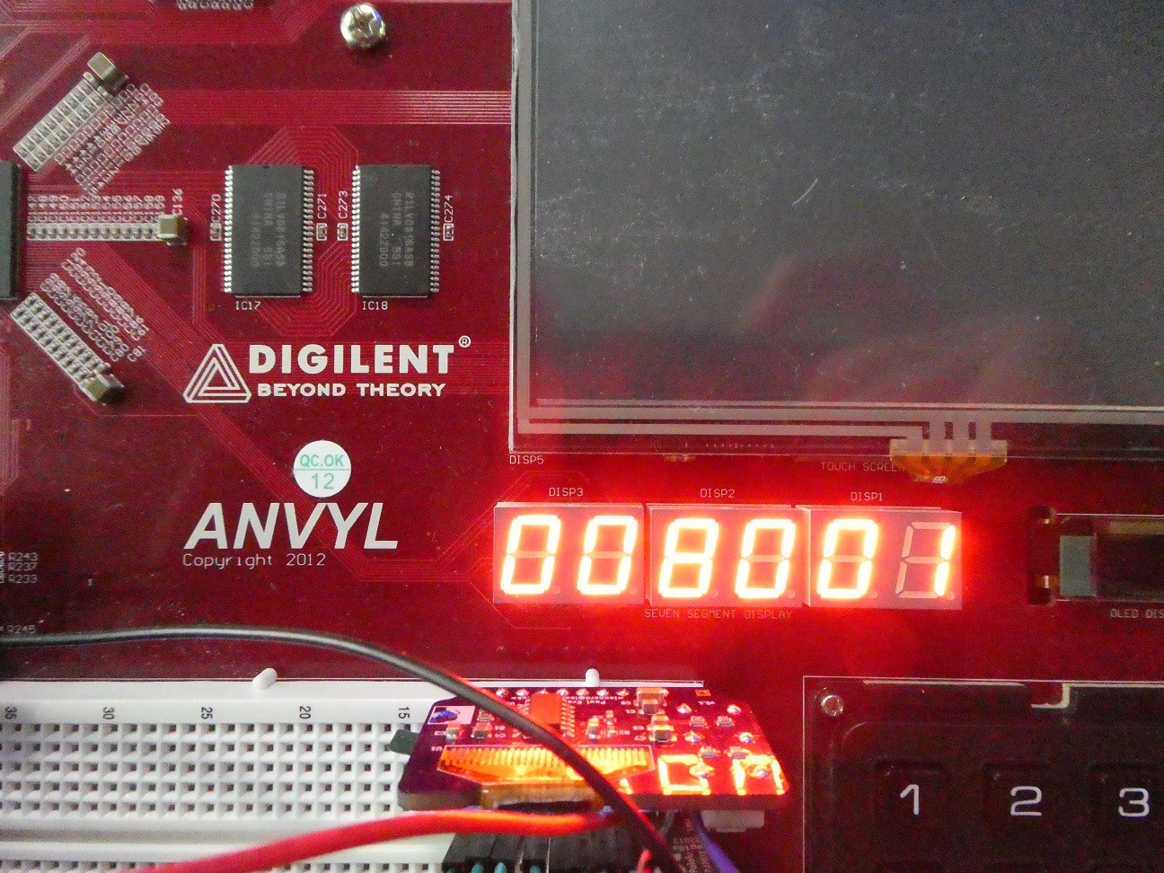
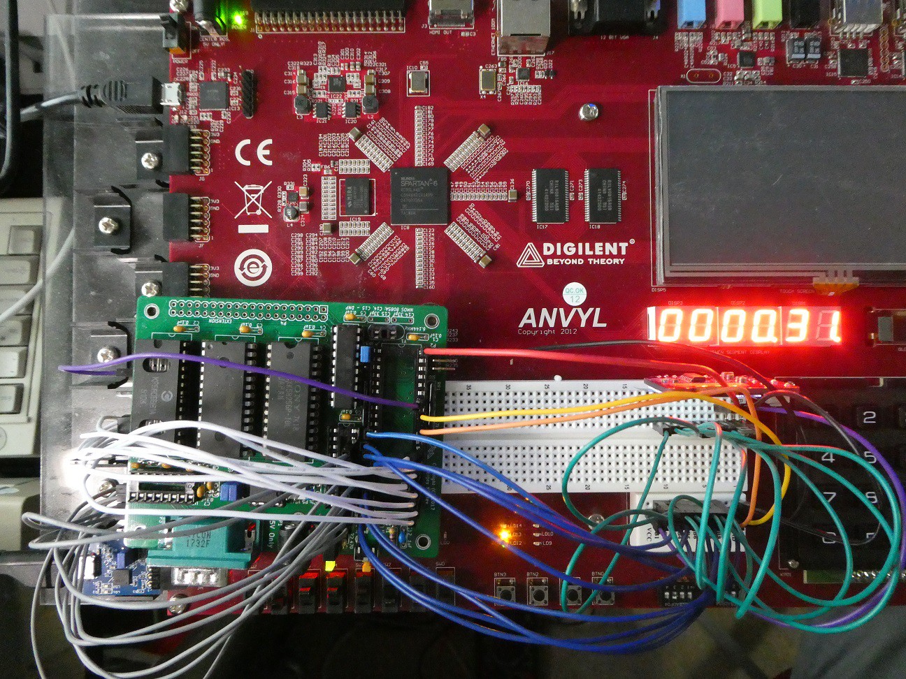
Turns out, with some breadboards, wiring, and bringing the Intel HEX component buses outside from FPGA into the physical world, the same components can be reused for a custom and handy testing tool.

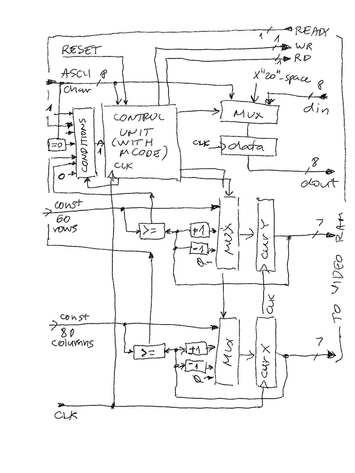
This testing allows to check:

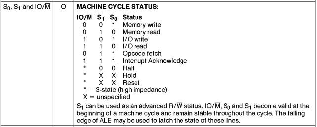
  • Address, data, some control (R/W) buses
  • (EP)ROM/RAM if populated (for expected content or read / write / re-read)
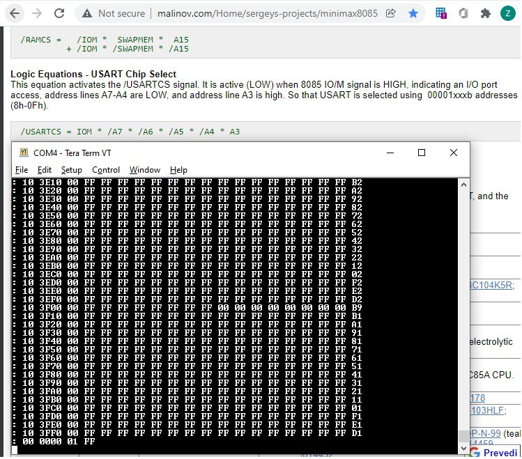
  • Address decode logic (e.g. mapping of ROM/RAM, repeats due to partial decode etc.)

Note that boards / computers tested this way do not need to be populated fully with ICs or other components, so it is possible to check "dead" or "not yet alive" boards too.

There are two possibilities:

  • CPU is not on the board, "insert" the wires into CPU socket (poor man's in-circuit emulator)
  • CPU is on the board, but there is bus access that allows DMA takeover (e.g. BUSREQ/BUSACK in Z80-type buses)

What cannot be readily tested using this approach:

  • Non-memory oriented bus signals (e.g. clocks, interrupts etc.)
  • I/O (memory mapped) - there can be indication that it "kinda works" as those spaces will be read as whatever default the I/O device returns, and in case of write in some simple case (e.g. write latch connected to some LEDs or relays) it may work.
  • I/O (separate) - with extra signal I/O space can be "forced" to appear as memory space and then it can be figured out if the data returned makes sense or not (example given below)

sys_dbg8085.bit

BIT file compiled for Digilent Anvyl board - machine cycle tracing

bit - 1.42 MB - 12/22/2021 at 17:52

Download

sys_sbc8085.bit

BIT file compiled for Digilent Anvyl board - HEX to mem, and mem to HEX

bit - 1.42 MB - 12/08/2021 at 04:43

Download

mcc.zip

Microcode compiler binary file (run mcc.exe -? for basic help)

x-zip-compressed - 71.72 kB - 12/08/2021 at 04:30

Download

test_0x0000.hex

Simple HEX file mapped starting at 0x0000 (for systems with RAM at low addresses, such as 6502, 6800, 6800, 9900, 1802)

hex - 1.03 kB - 12/08/2021 at 04:24

Download

test_0x8000.hex

Simple HEX file mapped starting at 0x8000 (for systems with RAM at high addresses, such as 8080, 8085, Z80 etc.)

hex - 1.03 kB - 12/08/2021 at 04:24

Download

  • 1 × https://digilent.com/shop/anvyl-spartan-6-fpga-trainer-board/ Digilent Anvyl board
  • 1 × https://digilent.com/shop/pmod-usbuart-usb-to-uart-interface/ USB to UART PMOD adapter
  • 1 × https://www.pololu.com/product/2564 3.3V to 5V step-up voltage regulator
  • 1 × https://www.tindie.com/products/leonerd/8-channel-signal-monitor/ Signal monitor (optional)
  • 1 × https://www.pololu.com/product/1702 Male-to-male jumper wires

  • Micro-coded controller deep-dive

    zpekic12/22/2021 at 20:35 0 comments

    In this project, instead of using a standard embedded processor and programming it to execute 3 tasks at hand (parsing HEX character stream, generating HEX character stream, and writing character stream to video RAM driving VGA), I created 3 independent micro-coded controllers, each tailored per task, and which can all operate in parallel. They can also be taken out of this project and dropped to any other needing that functionality. 

    Creating such controllers is possible in standardized way using mcc - microcode compiler. The simplest of these is the tty_screen which was up and running in one afternoon. Here are the suggested steps.


    (before digging in, reading this log could be useful to explain some microcoding basics and how they are leveraged in my standardized / parametric approach)

    Define a high-level / draft design

    It should be obvious that this is a custom memory access circuit, where the memory address is given by cursor X and Y positions which can go from 0..79 and 0..59 (for 640*480 VGA with 8*8 pixel font, actual VRAM address is A = 64Y + 32Y + X). Data written into the video RAM is either coming from ASCII char input, or from video RAM (in case of scroll). In the simplest case operation is VRAM[Y,X] <= char; X++; Of course when X reaches rightmost position, X <= 0; Y++; and when Y reaches bottom row image is scrolled up. There is also handling from CR, LF, CLS etc. (for example CLS is nested loop of X, Y: VRAM[Y, X] <= 0X20; (space)

    Few things to note:

    • no need to worry about the internals of the control unit - it will be auto-generated with all the right parameters
    • it is good to define all the registers and where they will get their values from (other registers, external inputs), or from some ALU operations
    • control unit will drive a conditions code MUX, because it eventually only consumes true/false at each instruction for executing either the .then or .else part - this conditions should be enumerated to find out if 4, 8, 16 or more will be needed
    • control unit and internal registers are driven by same CLK (rising or falling edge is not important, but typically should be same)
    • typically only the control unit consumes RESET, other parts can be initialized under microinstruction control
    • control unit drives itself and the rest of the design, via direct signals (e.g. RD/WR in this design) or selecting MUXs in front of registers ("RTL")
    • condition control bits can come from inside of the design (e.g. comparing registers with zero etc.) or outside (e.g. memory READY), or any logical combination of those
    • signal width are good to note, but can be changed, they are not reflected in microcode

    Define instruction register use and width

    For a classic CPU, IR holds the currently executing instruction from the program stream. This controller processes ASCII stream, so it is useful to define the IR as currently processed character. If we care about 7-bit ASCII, that means 7-bit IR loaded from input 8-bit data input (MSB can be ignored). If char == 0x00 (NULL), that means no character to write to V-RAM.

    Instruction register output is connected to mapper memory address (see here), defined as:

    // mapper size is 128 words (as 7-bit ASCII code is used as "instruction") by 6 bits (to point to 1 of 64 microcode start locations)
    // also generate all memory file formats. Note prefix: for .vhd, which is used to prepend to all generated aliases and constants
    // this way multiple microcoded controllers can coexist in the same project even if their microfield have same name
    .mapper 7, 6, tty_screen_map.mif, tty_screen_map.cgf, tty:tty_screen_map.vhd, tty_screen_map.hex, tty_screen_map.bin, 1;
    

     Looking at the generated tty_screen_map.hex file it becomes obvious that this is an auto-generated lookup table:

    : 01 0000 00 0A F5
    : 01 0001 00 0B F3
    : 01 0002 00 12 EB
    : 01 0003 00 0A F2
    : 01 0004 00 0A F1
    : 01 0005 00 0A F0
    : 01 0006 00 0A EF
    : 01 0007 00 0A EE
    : 01 0008 00 0A ED
    : 01 0009 00 0A EC
    : 01 000A 00 13 E2
    :...
    Read more »

  • Machine cycle level debugging

    zpekic12/19/2021 at 03:22 0 comments

    With the memory and I/O map looking good (see test approach in previous log), I decided to complete both MiniMax85 single board computers, expecting they would work.


    Well, they didn't :-(

    After exhausting all the usual simple debugging steps (voltages and frequencies as expected on the right pins, testing ICs outside as much as possible (e.g. the EEPROMs), or changing ICs - I have 2 of each major chips) I still could not find the reason why the SBC was completely unresponsive on the serial port.

    I decided to "re-wire" the FPGA to SBC for sort of custom "in-circuit emulator":

    • Move the CPU from SBC to FPGA breadboard
    • Wire one set of signals from breadboard to CPU socket on SBC (only those that are needed, for example SID/SOD etc. are not critical)
    • Wire another set of signals from CPU to FPGA. These include address, data, and some control signals - these are "read-only" for FPGA as it is only "listening" to the state of CPU signals and displays/logs them.
    • Drive CPU's READY signal - READY low puts the CPU in the wait state which can last indefinitely. During this time most control signals are in "frozen" state. 

    CPU is surrounded by wires, many pins have 2, one to SBC another to FPGA:

    Overall connection is messy, but works (including the 6.144MHz crystal which is pretty removed from CPU XTAL pins against all recommendations)

    With these connections, I went on to write a new FPGA design, with reusing much of the components I already had.

    The key idea is to:

    1. spy on the machine cycle appearing on the bus (IO/nM, S1 and S0 signals are used for this, refer to 8085 documentation)
    2. be able to select any (or none, so CPU runs at full speed) of machine cycles of interest, and if hit, drive READY low
    3. while READY is low, pick up the state of CPU signals of interest (address, data buses) and display them on VGA and serial terminal (reusing existing components)
    4. When all signals are displayed, wait for manual "continue" signal (simple button click, or it can be held down)
    5. Based on what is seen, figure out the bug

    1 - 4 above worked great (and that's why I am documenting as it can be useful for other hobbyists) but I failed at 5. I see the bug, but not yet sure what is causing it.

    In the boot sequence, jump to 0x010B is successful, but at that location CPU reads 0xFF (RST 7) instead of 0xCD (CALL) - RST 7 of course calls into interrupt vector entry point (0x0038) and executes that instead of the required init routine. The AT28C256 contains the right value at that address (as read by legendary TL866). I observe with simple volt meter (at this point all signals except CLK are frozen) /OE and /CS low, but all data bus high. 

    Bug or not, it is fascinating to observe CPU in action, going through its cycle exactly as it is described.

    Session with only instruction fetch traced (IO/nM & S1 & S0 = "011")

    And a session with all memory access traced (IO/nM & S1 & S0 = "0XX")

    The core of the design are 2 registers ("process" in VHDL parlance). The first register captures the machine state and trailing edge of ALE (same moment multiplexed AD bus has the address bits A7 .. A0):

    -- capture low address bus as ALE goes low
    on_ALE: process(ALE, DBUS)
    begin
        if (falling_edge(ALE)) then
            ABUS(7 downto 0) <= DBUS;
    --        "SBUS" is handy 3-bit indicator of the access;
            SBUS <= IOM & S1 & S0;
        end if;
    end process;

    Note that SBUS can only have 8 discrete states, as described here:

    These states are evaluated at each CPU clock cycle (which is also spied on by the FPGA) and rdy_ff (ready flip-flop) state updated:

    on_CPUCLK: process(CPUCLK, SBUS, reset)
    begin
        if (reset = '1') then 
            rdy_ff <= '1';
        else
            if (falling_edge(CPUCLK)) then
                if ((thaw and button(0)) = '1') then
                    rdy_ff <= '1';
                else
                    rdy_ff <= not switch(to_integer(unsigned(SBUS)));
                end if;
            end if;
        end if;
    end process;

    At RESET or when "thaw" (tracer has finished displaying the bus status record) or "continue"...

    Read more »

  • Operation mode 0 - Read memory contents and emit as Intel HEX format ASCII stream

    zpekic12/08/2021 at 05:47 0 comments

    The key component in this mode is predictably the Mem2Hex described here. This is how the component is hooked-up:

    hexout: mem2hex port map (
                clk => hex_clk,
                reset => reset,
                --
                debug => hexout_debug(15 downto 0),
                --
                nRD => nRead,
                nBUSREQ => hexout_busreq,
                nBUSACK => hexout_busack,
                nWAIT => nWait,
                ABUS => ABUS,
                DBUS => DIN,
                START => button(0),        
                BUSY => LDT1Y,            -- yellow LED when busy
                PAGE => page_sel,        -- select any 8k block using micro DIP switches
                COUNTSEL => '0',        -- 16 bytes per record
                TXDREADY => tx_ready,
                TXDSEND => hexout_send,
                CHAR => hexout_char
            );

    Few notes:

    • I copied the VHDL and microcode (split) because I expected more changes to do to the design, but in the end they were mostly cosmetic. 
    • clk (IN) - 12.5MHz, but this is not critical, it can go from 0 to 50MHz.
    • reset (IN) - Anvyl has no "hardware reset" button, so pressing all BTN together is a "reset"
    • debug (OUT) - state from microcode controller driving the design is output and can be shown on 7seg LED (useful to single step through microcode)
    • nBUSREQ (IN), nBUSACK (OUT) - Z80 syle DMA signals.
    • nWait (IN) - there is a common WAIT state generation circuit shared by Mem2Hex and Hex2Mem (described above)
    • ABUS (OUT), DBUS (IN) - connected to outside world, along with nRD
    • START (IN) - triggered manually (see my finger on the button in video below :-) )
    • PAGE (IN) - original component supports selecting any combination of 8k pages. I ran out of switches so I combined 2 bits per DIP to configure the memory to be output, so it is 16k blocks ("page_sel")
    • COUNTSEL (IN) - allows 16 (0) or 32 (1) bytes per record.
    • TXDREADY (IN) - handshake signal for character output. Microcode waits for this signal to go high before next character is emitted. 
    • TXDSEND (OUT) - if TXDREADY is high, then a character is put into outside buffer and this signal driven high. The UART par2ser implements the reverse side of this protocol. A FIFO could be injected between them.
    • CHAR (OUT) - ASCII code of the HEX stream generated appears here.

    Here is how the send character handshake appears in the microcode:

            // "UART" is supposed to signal TDXREADY = 1 when presented 0x00 or when serial trasmit is done
    emit:        if TXDREADY then next else repeat;    // sync with baudrate clock that drives UART
            if TXDREADY then next else repeat;
            if TXDREADY then next else repeat;
            if TXDSEND then return else return;

     TDXREADY is checked 3 times in a row to prevent any clock domain glitches. Finally, the TXDSEND is checked, but this condition is hardcoded to "1", means it will always return to the caller at this point, but a simple comparator is hooked up to look for check of this condition to generate the send pulse:

    -- hack that saves 1 microcode bit width
    TXDSEND <= '1' when (unsigned(m2h_seq_cond) = seq_cond_TXDSEND) else '0';


    Sanity check for I/O:

    Reading the I/O space can give some indication if it "sniffs right", like in this case. The only IC hooked up to I/O space is 8251 UART, which is enabled when address is XXXXXXXX0001XXXX - when dumping out addresses that match it is visible that "something" appears in those locations, while everywhere else the DBUS returns the default float high. 

  • Operation mode 1 - Parse ASCII stream in Intel HEX format, and write to memory

    zpekic12/08/2021 at 05:32 0 comments

    The key component here is Hex2Mem which I intend to document better on its own page. But few explanations here until I get around to do it. Refer to slightly modified VHDL and microcode

    Basic operation is as follows:

    1. Wait for ASCII character
    2. If there is one, branch to location that processes it (the ASCII code can be thought of as an "instruction")
    3. If invalid, output error, go to step 1
    4. If valid, process it based on which it is and what is expected or not (for example ":" can come only once at the beginning of line, spaces or tabs anywhere but will be ignored, unless they are between hex digits that should not be split (e.g. data bytes)
    5. Each two digits are written into one internal byte memory location (there is a small 64 bytes buffer)
    6. As a byte is written into internal RAM, the checksum is updated
    7. The number of bytes received is checked with expected record length, for error check
    8. Final byte received is the checksum. Added to accumulated checksum it should result in 0x00 in the LSB of the checksum register
    9. If checksum is correct, the data bytes are written in a burst to external RAM bus. This means RAM will not be thrashed by bad checksum record
    10. Either CR and/or LF indicates end of record, this increments the line counter, clears the character counter (these are only used to show error message) and processing of new record can start.

    This is how it is hooked up into the design:

    hexin: hex2mem Port map (
                clk => hex_clk,
                reset_in => reset,
                reset_out => open,
                reset_page => page_sel, -- not really used but i8080-like system would reset at lowest 8k updated
                --
                debug => hexin_debug(15 downto 0),
                --
                nWR => nWrite,
                nBUSREQ => hexin_busreq,
                nBUSACK => hexin_busack,
                nWAIT => nWait,
                ABUS => ABUS,
                DBUS => DOUT,
                BUSY => hexin_busy,    -- yellow LED when busy
                --
                HEXIN_READY => hexin_ready,
                HEXIN_CHAR    => hexin_char,
                HEXIN_ZERO => open,
                --
                TRACE_ERROR => dip_traceerror, 
                TRACE_WRITE => dip_tracewrite, 
                TRACE_CHAR    => dip_tracechar, 
                ERROR => LDT2R,    -- red LED when error detected
                TXDREADY => tty_sent,
                TXDSEND => hexin_debug_send,
                TXDCHAR => hexin_debug_char
            );

    Signals:

    • clk (IN) - common 12.5MHz, can be virtually any speed, but fast enough to be able to keep up with incoming baudrate
    • reset_in (IN) - classic reset
    • reset_out (OUT) - will generate a pulse if write is detected to any of the "reset_page" 8k blocks. Typically this would be 0x0000 - 0x3FFF for "PC starts at 0" CPUs (808X, CDP1802), and 0xC000 - 0xFFFF for "reset vector" CPUs (65XX, 68XX, 99XX)
    • reset_page (IN) - 8 bits, each indicates 8k block
    • debug (OUT) - signals from microcode controller unit, useful for single stepping through microcode
    • nWR (OUT) - Z80 style memory write signal
    • nBUSREQ (OUT), nBUSACK (IN) - DMA signals. The first time nBUSREQ will be generated when a valid HEX record has been received. At that point, memory write can be allowed if nBUSACK goes low. Which will only happen if operation mode is this one.
    • nWAIT (IN) - see description below
    • ABUS (OUT), DBUS (OUT) - connections to system bus (in this case, wires to 8085 SBC board)
    • BUSY (OUT) - blinkenlight :-)
    • HEXIN_READY (IN) - connected to UART, when a valid serial character is received, UART generates which pulse which captures the received character to process.
    • HEXIN_CHAR (IN) - 8 bit ASCII character from input stream
    • TRACE_ERROR, TRACE_WRITE, TRACE_CHAR (IN) - 3 independent switches that enable tracing when error, when writing to memory or when character is received. These are simply conditions for microcode, if true then execution branches to tracing (output of a text string). This is a fundamental advantage of microcoded designs as the debug facility can be written along (or best - before) the rest of the design / code!
    • ERROR (OUT) - red blinkenlight!
    • TXDREADY (IN), TXDSEND (OUT), TXDCHAR (OUT) - these are connected to TTY which allows tracing to be shown on VGA. Note that writing to VGA still takes some time so the input stream should be delayed by character or line when extensive tracing...
    Read more »

  • Test mode 2 - display UART baudrate and host to TTY/VGA loopback

    zpekic12/08/2021 at 05:26 0 comments

    Another test mode which:

    • Displays real baudrate (BCD format) on the LEDs
    • Also provides character loop-back just like mode 3

    Anvyl switches SW5..3 select the baudrate from 600 (000) to 57600 (111). Note that the number displayed is not exactly the typical standard rate. The reason is that the frequency is actually measured on the board. First, the FPGA 50MHz board frequency is divided by two prescale factors, one leads to freq_4096 that can be divided by powers of 2 down to 1 Hz, and the other based on the selected divide value to get baudrate_x8 frequency:

    prescale: process(CLK, baudrate_x8, freq4096, switch_uart_rate)
    begin
        if (rising_edge(CLK)) then
            if (prescale_baud = 0) then
                baudrate_x8 <= not baudrate_x8;
                prescale_baud <= prescale_value(to_integer(unsigned(switch_uart_rate)));
            else
                prescale_baud <= prescale_baud - 1;
            end if;
            if (prescale_power = 0) then
                freq4096 <= not freq4096;
                prescale_power <= (clk_board / (2 * 4096));
            else
                prescale_power <= prescale_power - 1;
            end if;
        end if;
    end process;

    Eventually these two are used to feed into a counter that counts in BCD (more precisely, it has a 32-bit adder inside that can add in BCD or binary):

    counter: freqcounter Port map ( 
            reset => RESET,
          clk => freq_2048(11),
          freq => baudrate_x1,
            bcd => '1',
            add => X"00000001",
            cin => '1',
            cout => open,
          value => baudrate_debug
        );

     The counter assumes that the "clk" signal is 50% duty cycle, as it has 2 counters which work on opposite sides of the clk level. Counts accumulated on "high" side are displayed on "low" side and vice versa, with the net result that each 1s the count ("freq" signal) is refreshed. Because 50MHz cannot be divided by some integer to create exact baudrate, they are off by less than <1% which is of course well within timing tolerances. 

    This way the crucial UART frequency generation, LED debug display etc. are tested. 


  • Test mode 3 - display UART mode and host to TTY/VGA loopback

    zpekic12/08/2021 at 05:17 0 comments

    To have confidence in a test circuit, it is useful for the test circuit to test itself :-) This mode:

    • Displays the UART mode in somewhat cryptic way in 6-digit 7-seg LED

    UART is two separate circuits (SER2PAR and PAR2SER) that I reuse in many projects. They support a variety of 8-bit per character transmit and receive frames. The terminal program on the host should be set to same setting (8-N-1 in this case)

    Anvyl board switches 2..0 select the mode as visible in the image below.

    (note 700ms delay per line - this is to allow time for the trace of HEX2MEM microcode to display before processing next incoming character, more about this below)

    • Echos the characters coming from UART input (RX) back to output and also to TTY2VGA. This allows testing those components too. 

    To simplify top level object, the TTY, video RAM, chargen RAM and VGA controller are wrapped up in one component called TTY2VGA:

    • VGA mode: 640*480, 25MHz pixel clock
    • Text mode: 80*60 characters, 8*8 pixels
    • Video RAM: 4k, dual port. The port connected to TTY controller is read/write (read is used when scroll-up is needed, this is of course a bad design as a top-row register pointer could allow using write on that side) and the port connected to VGA controller is read only. Both ports take x, y (row/col) and internally a hardware "multiplication" is done to find out the character code address (A = Y*MAXCOL+X)
    • Character generator ROM: 128 characters (0-127 ASCII, 128-255 are simply inverted in the circuit), total of 1k
    • Hardware cursor in two modes (underscore and block)
    • Color is hard-coded but could easily be extended by addition of 4k color RAM, similar to video RAM

  • Software

    zpekic12/08/2021 at 05:08 0 comments

    There are 3 different toolchains and languages coming together in this project:

    • Intel HEX file - there are innumerable systems and tools producing and consuming this old but still useful format, most notably all the assembler, cross-assemblers etc. in 8080/Z80 ecosystem on one side, and bunch of programmers, emulators etc. on others. Any can be used in combination with this project - as long as it is "old enough" (producing just 64k address space and 00 and 01 type records only)
    • VHDL (using Xilinx ISE 14.7) - to compile it all together and generate a .bit file, standard FPGA toolchain flow. Few notes:
    • Microcode - this is custom "language" I "invented" to simplify creating templatized controllers. There are 3 such microcoded controllers in this project:
      • HEX2MEM - accepts stream of ASCII characters, interprets them as valid Intel HEX file stream, and generates memory write signals
      • MEM2HEX - generates memory read signals, bytes read are assembled into Intel HEX file output ASCII stream
      • TTY_Screen - accepts ASCII character stream (including some special characters such as CR, LF, CLS, HOME) and writes into a memory organized as MAXCOL columns and MAXROWS rows (in this project 80*60 for a text based VGA, but could for example be a 16*4 LCD etc.)

    The software components are best explained by going through the 4 supported modes of operation:

    ---------------------------------------------------------------------------------------------            
    --     SW7    SW6    Mode                TTY (VGA)            UART TX                7seg LED    
    ---------------------------------------------------------------------------------------------
    --        0        0        sel_hexout        -                         Generated HEX        mem2hex debug port (or bus if nWait = 0)
    --        0        1        sel_hexin        Microcode trace    Echo UART RX        hex2mem debug port (or bus if nWait = 0)
    --        1        0        sel_loopback0    Echo UART RX        Echo UART RX        Baudrate (decimal)
    --        1        1        sel_loopback1    Echo UART RX        Echo UART RX        UART mode    
    ---------------------------------------------------------------------------------------------

    See other project logs for description of each of these modes of operation.

  • Hardware

    zpekic12/08/2021 at 05:03 0 comments

    For this project I used a cool little 8085-based single board computer (8085 Minimax) described and graciously provided to me by Ken Yap (thanks again!). I was actually in the process of soldering together the board, and decided to use a verification step before plugging in my vintage Soviet CPU to see if there will even be a chance for it working or not...

     The hardware setup is simple but a bit messy affair:

    Few notes:

    • 8085 IO/M signal (purple wire) is simply switchable to IO (high) to M(emory) (low) using a micro-DIP on the FPGA board. The HEX I/O has no idea about it, it just sees IO space as another 64k address map space (of course with 256 repetitions because typically in 8080-family systems upper 8 address lines are not decoded (Z80 introduced 16-bit IO to some degree, and then HD64180 has a full 64k IO address map)
    • 8085 has multiplexed lower address A7..A0 with data bus D7..D0, giving AD7..AD0 bus. Typically a 8-bit latch (like 74x573) enabled by ALE captures the low address early in memory access cycle. To simplify, I left this IC unpopulated on the board and connected the low memory address wires (gray) directly to its output socket pins.
    • Minimax 8085 of course takes +5V DC - I am sourcing its modest consumption (esp. because the power hungry NMOS CPU is not there!) with a 3.3V to 5V step-up regulator
    • Connecting nominal 3.3V (FPGA) to nominal 5.0V (SBC) is a "circuit crime". But I could get away with it in this case as the modern RAM / ROM used has max "0" voltage and min "1" voltage signals that are within margins.
    • 4 additional PMOD signals are used for UART - this is how the Intel HEX files are uploaded/download during runtime.  

    This is how these connections look in VHDL (top file of the project):

                    --PMOD interface
                    JA1: inout std_logic;    -- Connected to USB2UART
                    JA2: inout std_logic;    -- Connected to USB2UART
                    JA3: inout std_logic;    -- Connected to USB2UART
                    JA4: inout std_logic;    -- Connected to USB2UART
                    JB1: out std_logic;    -- GRAY 74F573.19 A0
                    JB2: out std_logic;    -- GRAY 74F573.18 A1
                    JB3: out std_logic;    -- GRAY 74F573.17 A2
                    JB4: out std_logic;    -- GRAY 74F573.16 A3
                    JB7: out std_logic;    -- GRAY 74F573.15 A4
                    JB8: out std_logic;    -- GRAY 74F573.14 A5
                    JB9: out std_logic;    -- GRAY 74F573.13 A6
                    JB10: out std_logic;    -- GRAY 74F573.12 A7
                    JC1: out std_logic;    -- WHITE 8085.21    A8
                    JC2: out std_logic;    -- WHITE 8085.22    A9
                    JC3: out std_logic;    -- WHITE 8085.23    A10
                    JC4: out std_logic;    -- WHITE 8085.24    A11
                    JC7: out std_logic;    -- WHITE 8085.25    A12
                    JC8: out std_logic;    -- WHITE 8085.26    A13
                    JC9: out std_logic;    -- WHITE 8085.27    A14
                    JC10: out std_logic;    -- WHITE 8085.28    A15
                    JD1: out std_logic;    -- PURPLE 8085.30 IO/M (low for memory access)
                    -- breadboard signal connections
                    BB1: inout std_logic;    -- BLUE 8085.12 AD0
                    BB2: inout std_logic;    -- BLUE 8085.13 AD1
                    BB3: inout std_logic;    -- BLUE 8085.14 AD2
                    BB4: inout std_logic;    -- BLUE 8085.15 AD3
                    BB5: inout std_logic;    -- BLUE 8085.16 AD4
                    BB6: inout std_logic;    -- BLUE 8085.17 AD5
                    BB7: inout std_logic;    -- BLUE 8085.18 AD6
                    BB8: inout std_logic;    -- BLUE 8085.19 AD7
                    BB9: out std_logic;        -- ORANGE    8085.31 nWR
                    BB10: out std_logic;        -- YELLOW    8085.32 nRD

View all 8 project logs

Enjoy this project?

Share

Discussions

Similar Projects

Does this project spark your interest?

Become a member to follow this project and never miss any updates