 Sleepy Pony
Continues from Part 1
Chip Enable
To communicate with DS1302, we need to hold the Chip Enable (CE) signal high throughout the transaction and return it to low after the transaction ends. So in this part of the circuit, I OR the enable signal from all three types of the signal together to enable the SCLK and CE signals.
Note: This circuit is part of the SPI bus arbitration circuit which is not in full working order yet at this point of writing, so pin 13 of U3 is force high for the time reading part to work.

Time Burst Read Command
We need someplace to store our time burst read command (0xBF). In this case, I choose a 74HC165 Parallel-to-Serial Shift Register for this job. By being a shift register it works like a typical SPI bus, and by having a parallel-load feature we could set the value we need as a parallel input and load it into the register each time we start the transaction. Perfect.

In Or Out?
SPI is actually an easy protocol to make a logic circuit for. You generally just need a clock source and two sets of shift registers connecting in a circle. However, DS1302 complicates that by sharing MOSI and MISO pins. This forces us to control the data direction in and out of the chip according to the number of clock pulses that already passed: output for 8 pulses and then input for 64 pulses.
Luckily, the step counter CD4040 we use to count 72 pulses of SCLK breaks out every counting bit out, so we can tap the counter at the 9th pulse to switch the data direction.
To switch the direction, we will use a 74HC125 Tri-State Buffer. This kind of buffer is convenient when we need to isolate one part of the bus from another just by disabling the buffer. Here, we use it to isolate the command store register from the SDIO pin after 8 bits of command were sent.
Note: This circuit is part of the SPI bus arbitration circuit which is not in full working order yet at this point of writing, so pin 1 and 4 of U3 are force high for the time reading part to work.
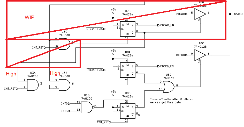
To summarize this part of the circuit which is probably the most confusing part, first, the ~RTCRD_TRIG signal from the time read timer will cause the command store U24 to load 0xBF into the register on the falling edge, then on the rising edge, U8A will latch high, causing the RTCRD_EN signal to go high which in turn causing the CE signal to go high and also enable the SCLK clock.
At this time U5C will output low, enabling the tri-state buffer U10C which will allow 0xBF to pass to the SDIO pin. At the 9th rising edge of SCLK however, CNT0 and CNT3 signals will both go high (2^0 + 2^3 = 9) and set the U8B flip-flop to high. This will disable the U10C buffer to allow DS1302 to output data onto the bus. SCLK will continue for 64 more cycles before the ~CNT_RST signal goes low and reset everything back into the initial state.
Storing the Output
DS1302 should output the date-time data on the bus at this point. We will need 8 bytes of storage to store the data before we could output it to the display. I choose to use 8 of 74HC595 8-Bit Shift Register with Tri-State Output Registers. There are many aspects of this popular chip that makes it perfect for our use case.
- The outputs are Tri-State, which means we could choose to enable one specific chip to output at a time, making multiplexing the output at the display easy.
- The outputs are also buffered. We can freely shift the data into the chips and then latch the data to the output when we are ready. The shifting action will not be seen on the outputs.
- The chip can be chained together, and all output bits are available for use.
Here you can see the registers are chained together into a big 64-bit register. The data input pin SER is connected to the SDIO signal. Shift clock SRCLK is connected to SCLK, and output latch clock is connected to RCLK signal, which is actually CNT_RST signal i.e. that data will be outputted when the 72nd clock pulse was reached.
Additionally, the Output Enable (~OE) pins of the registers are pulled down and connected to a pin header. This will enable the output on all chips by default. We can disable some of them (or let only one enabled at a time for multiplexing) by driving the OE signal high.

In the next log, I will talk about the 7-segment display board which is the last part that is currently finished. Thanks for reading this far!
Discussions
Become a Hackaday.io Member
Create an account to leave a comment. Already have an account? Log In.