 Adrian Freed
555 Core
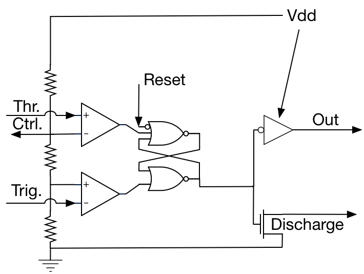
The first step for 20-pin 555 timers is to improve the timer core itself.
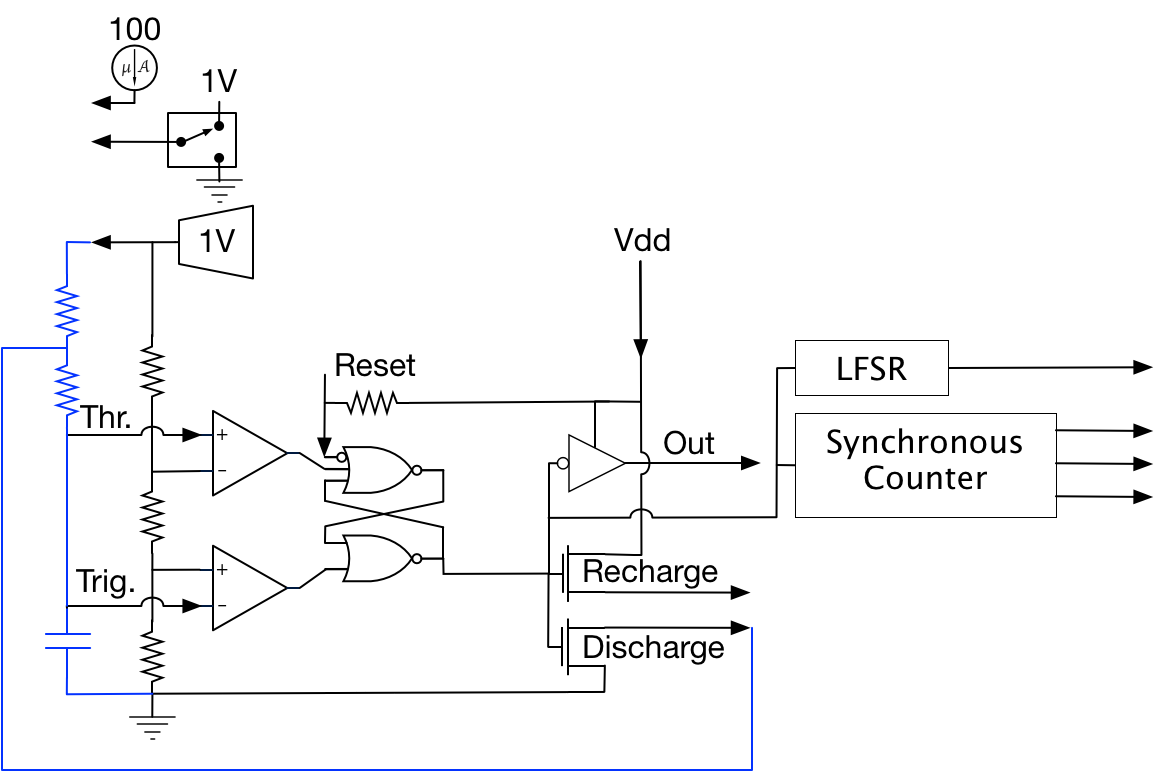
Recharge Pin
Adding a recharge pin driven by the same source as the existing discharge pins opens up some interesting possibilities.
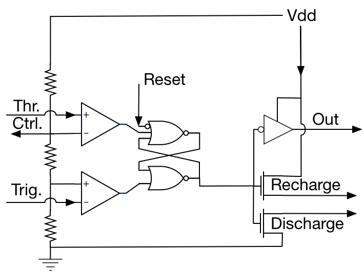
For the simple RC oscillator driven from the output pin, two pins are now available to drive LED’s which will flash alternately. This oscillator will be relatively stable as the timing components are not sensitive to the loads on these separate output transistors.
If instead we charge and discharge the capacitor with these pins we can use a potential divider or potentiometer to set the mark to space ratio of the output of the timer
We can also short all three output pins together to increase drive capacity.
Pull Up on Reset Pin
A pull-up resistor on the reset pin prevents strange behavior when the pin is left disconnected.

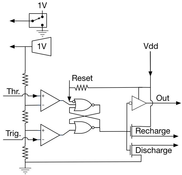
Band Gap Voltage Reference Pin
The 555 timer is a kit of general analog and digital parts connected internally for timer and oscillator applications. We see these components everywhere in modern IC’s: comparators (e.g. sense amplifiers in memories), flip-flops (the basis of SRAMs and CPU registers), and high-power output buffers (e.g., class D audio). Fifty years ago there wasn’t pin-count or budget for a component that is now ubiquitous alongside these building blocks: the Band Gap Voltage Reference.
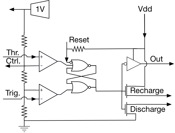
Replacing the voltage source of the divider network and R/C network with a 1V reference improves on the original 555 by further isolating the time constants established by these networks from changes in the power supply. The usual simplified analysis of 555 timer sensitivities doesn't take into account the difference between the two current legs: the external one which integrates all fluctuations in the power supply during a cycle and the internal one where comparators only sample the divided power value at a particular point in the cycle. This makes the timing sensitive to glitches and noise on the power supply - something that is mitigated if the currents are sourced from a voltage reference.
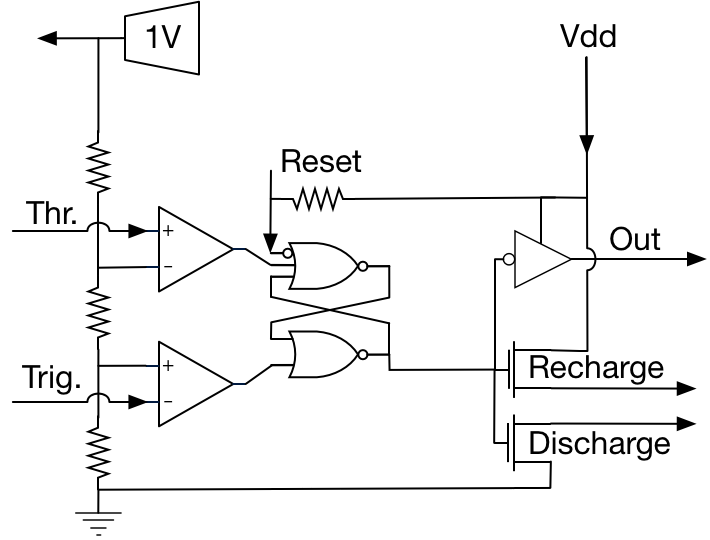
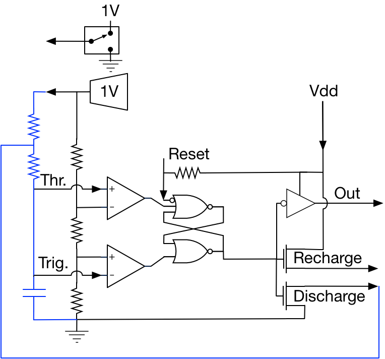
One less Pin
Another source of noise can be avoided by removing the external connection to the resistor divider network. This pin is mostly used for frequency, pulse width or pulse position modulation which can be achieved in another way: The 1V timing source lowers the timer trip voltages (1/3V, 2/3V). This means that very wide timer modulations can be achieved with external currents applied directly to the charging capacitor.
1V push-pull Output Pin
A popular astable circuit uses a single resistor on the output. By providing an additional output that switches between ground and the 1V reference, this astable with 50/50 mark to space ratio can be easily achieved freeing up the full swing output pins from timing duties.
Constant Current Source Pin
We can restore the function of the 9th pin originally cut from the 555 timer design: a constant current source - in this case 100uA. This source produces a linear ramp on the charge capacitor and a sawtooth waveform - without additional components.
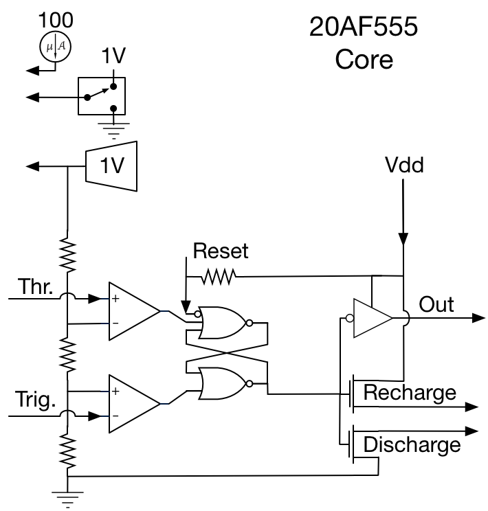
Core Summary:
- 4 more pins: Constant Current, 1V, 1V push-pull, recharge
- 1 less pin: Modulation input
- This leaves 9 available pins in a 20-pin package.
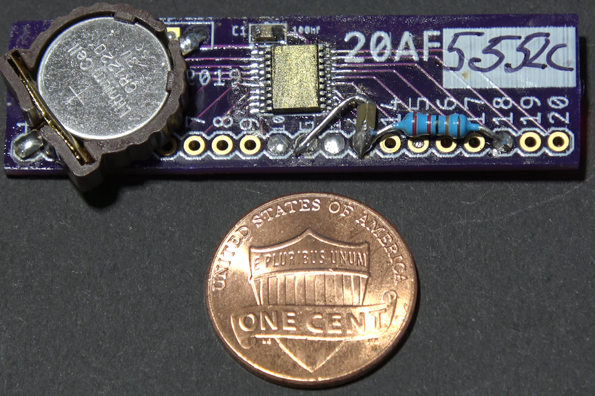
The core itself is relatively small in modern CMOS processes and sophisticated CAD tools are used that allow for reuse of cores. Many application-specific variants using the core can be made economically thereby reducing the risk of betting the company on a single design. The 555 timer was the only major hit of the handful of other important related IC’s designed at Signetics.
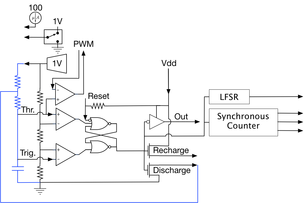
Here are two different bespoke designs intended for circuits where the 555 core is configured as an oscillator.
20AF555LC - For Light Chasing and Sequencing
A very common introductory electronics kit connects a handful of LEDs, a 555 timer and a ring counter to make a light chaser. By presetting the first flip flop of a shift register, a high value can be propagated along eight buffered outputs. So to circulate this single high value the last stage can be connected back to the input of the shift register. Shorter circulation patterns are easily achieved by connecting the input to an earlier output of the shift register.
Complementary Outputs from an additional flip flop allow for multiplexing 2 arrays of LED’s producing a 16-LED chaser.
20AF555WF - For WaveForm Synthesis
Instead of using all the remaining pins for a single function of the clock, the WF variant provides many single output variations useful in waveform synthesis applications.
LFSR
A linear feedback shift register produces a long pseudo-random sequence which at high frequencies is a useful audio frequency noise generator.

Synchronous Counter
A flip-flop divider will produce a clean square wave at its output. Dividing the output from this divider by two further dividers creates a binary counter or suboctave signals that can be mixed and combined to synthesize staircase waveforms. A synchronous counter implementation performs the same function without accumulated delays with only a handful of extra gates.
PWM
The addition of a third comparator connected internally to the charge node implements a voltage controlled PWM output - for audio amplifier or motor speed control applications.
APC
A simple RC monostable triggered by the 555 core affords independent control of pulse width and pulse rate - the basis of the APC - “Atari Punk Console” sound.
More 555 Goodness
These two chips emphasize using extra pins to give more flexibility and generality to the 555 timer. What if we already know how we want to configure the 555 timer and want as many pins of the 20-pin package as possible freed up for another function? That story is explored in another project.