 Dave Collins
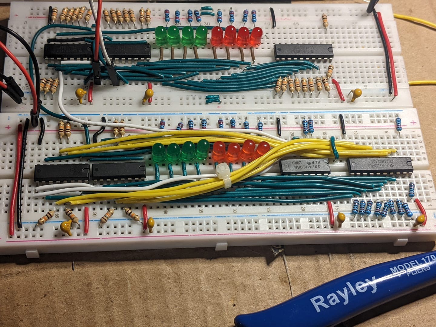
I've completed building up both the data bus storage, and the accumulator registers. Both designs were developed to be very similar to the Ben Eater / SAP - 1 style register module. The two registers are slightly different, so I thought i'd try to explain my thought process here for each of them.
Bus Control
Each is separated from the main bus with a SN74HC245E bus transceiver; which is used to enable the register output.
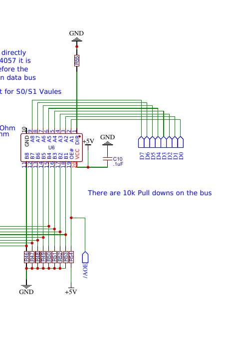
A logic low signal is required by this package's output enable that will likely require an inverter to control the signal from the module handling the micro-coded instruction set; as its likely the EEPROM may have an issue driving the signal low, even with the weak pull-up. This will need to be a consideration for that module when I finally get around to building it. On the accumulator (pictured above) the data bus is only connected to the transceiver output, however on the storage register it is connected to both the transceiver output and the input of the d-latch which is used in that module. This was done, as the CD4057 has an internal shift register which can only be updated by the ALU via a control word; it is not directly wired to the bus. The Data storage register however is, and can be updated via the main bus or output its contents onto the bus. I've tied the direction in a fixed state B -> A, and tied the output by default to high Z, so that when the /AOE or /BOE signals are not present from the control module the register is in high Z. Additionally input enable signal on the storage register must also be enabled for the register to accept a clock tick, so when it is not enabled the register is effectively in tri-state.
Latch package types:
The latches for the registers themselves are either constructed from 74HC194E universal 4 bit shift registers, or 74HC175E quad D-Latches. The a pair of shift registers make up the accumulator:
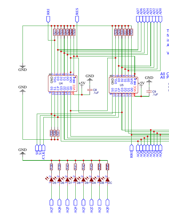
This will require some decode logic on the part of the ALU to set S0 and S1 (which change the store or shift function of the register. Additionally, other logic will be required to detect and return a carry bit in the case of a rotation operation. currently this is built as an eeprom; but the logic is so simple I may switch to building this as discrete logic; or a low pin output high speed prom. The advantage to using a shift register is that it saves on states in the eeprom for handling the rotation and shifting functions, as well as drastically simplifying the truth table. The B register on the other hand, uses a pair of quad d-latches and an and gate:
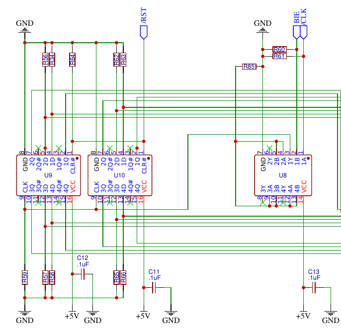
An enable signal was added by a logical AND gate with the falling edge of the clock. This allows the register to simply drop the clock pules which are not significant to updating the latch allowing us to simply attach the main bus directly to the latch. This was necessary as the quad d-latch always outputs its stored value, and always updates on the rising edge of what ever clock pulse comes in. Lastly updates to this register will be through the system bus and configured by the control module.
Conclusion and what's next:
Now that the registers are set up, we are ready to move on to the actual ALU and a very rudimentary control logic. As always I've updated the complete schematics of what I'm working on, and those can be located in the files section of the hack a day page. For more updates, you can always watch this space or check out the myriad Facebook groups I frequent. Particularly Minimalist Computing, lately. I hope you all had a pleasant week, and I hope to update this space with more as more details reveal themselves.
Discussions
Become a Hackaday.io Member
Create an account to leave a comment. Already have an account? Log In.