 Paul McClay
First posted to TekScopes at groups.io in several installments; here consolidated, with a few pictures added, and lightly edited.
Introduction
Put the kettle on. Here follows a long story about fixing a Tektronix 5A26 dual differential amplifier plugin, one of many different plugin modules for Tek's 5000-series oscilloscopes. Tek sold the 5xxx scopes from 1971 to 1991 and these plugins starting in 1976. Numbers that look like date codes suggest this unit was assembled in Q2 1980. They're kind of like old sewing machines: still useful and heartwarmingly fixable. If this sort of thing floats your boat, you might like #Tektronix 5D10 digitizer in 5441 (5440,5403) scope too.
NOTICE/spoiler: most of what follows turns out wrong in the end. If you got here by way of a search for information, maybe start at the end and read backwards!
Chapter One
This may be a unique fault and not directly useful for any future reference, but sometimes I enjoy reading how someone worked through a problem. Maybe someone will like to read this.
I bought a 5A26 dual differential amp "as is" from grainy photos that showed little except that it was not perfectly clean. So I get to take what I got and like it.
All the pushbuttons were terribly stiff or not functional at all. No big surprise and solved with solvents. Access to the bandwidth limit switches required some disassembly, which required some desoldering, but that much was well enough described in the manual and no big deal.
There were some glops of dried goop on the faceplate and a couple of the BNCs had more corrosion on them than I wanted to compact into whatever I might connect to them. Cleaning that up turned into a round of disassembly, cleaning, breaking, fixing, and things that could have been easier if I knew what I was doing. I might write more about some of that another day as a B-side to this.

It worked pretty well, if not perfectly calibrated, in dual trace mode or when displaying channel 2 only.
The "interesting" part was that when displaying only channel 1 it showed two vertically separated but otherwise identical traces. At slower sweep rates, it was clear that the two copies of ch1 were generated by ALTernation or CHOPping as if the plugin was displaying both channels. Also the same when combined with one or two traces from another plugin: with the 5A26 set to display ch1 only and a second dual trace plugin installed, the scope cycled through two traces from the other plugin and two identical but offset copies of ch1, by alternation or chopping, as though it were cycling through four traces from two dual trace plugins. With the 5A26 in dual trace mode the scope cycled normally through four legit distinct traces. Channel 2 worked normally, either by itself or in dual mode with ch1.
Chapter Two
So the displayed voltage of channel 1 was shifting with trace alternation.
The rest of this will make more sense with reference to "output amplifiers <2>" schematic:

I don't have a plugin extender. Of course the output stuff is on the right side of the plugin, not accessible through the left side of the scope frame. So diagnosis continues by pulling out the plugin, clipping leads onto points of interest and replacing the plugin in the left slot with leads hanging out from the empty right slot. Repeat.
I set the ch1 inputs to GND and ran a sweep slow enough to see the alternation.
Of course output voltage between the drains of Q282/Q292 changed with alternating sweeps. The drain of Q282 was steady and Q292 alternated. So that narrowed it down a bit. The emitters of Q242 & Q252 were both steady 19.4V, as indicated on the schematic. The difference between collectors of Q260 & Q270 alternated with Q260 steady and Q270 alternating. Q242 & Q252 drive the bases of Q260 & Q270, so at Q270 the base is right and the collector is wrong.
FETs Q282/Q292 handle channel switching by connecting/disconnecting the ch1 outputs to/from the mainframe interface board. They were clearly disconnecting ok because ch1 was off when it was supposed to be off. When "on", the source and drain of Q292 tracked each other, so it was connecting ok when ch1 should be connected. When displaying ch1, diodes CR283 & CR293 are back biased, which should isolate the ch1 signal from any influence by the channel switching logic. Puzzle.
Oh yeah... remembered the mainframe shorts the two channels together, connecting the drains of Q292 & Q392 and bringing ch2 into the picture.
Which should have no effect because when ch1 is on, Q_3_82 & Q_3_92 are off and, apart from bringing R394 into parallel with R294 that should do nothing to ch1-. And Q382 (ch2+) was switching off and the same signal switches Q382 & Q392. And Q392 responds correctly to that signal in dual trace mode. Puzzle.
It wasn't clear how the channel switching circuit could produce this result. Reviewing assumptions... was this really synchronous with ALT/CHOP logic? Seemed pretty clearly so. Could that timing come from anywhere but the timebase? The CHOP clock comes from the interface board, but the timebase clearly has control over CHOP vs ALT and the ALT timing can't come from anywhere but sweep timing. How could CHOP/ALT timing affect the plugin? The B21 CHAN SWITCH SIGNAL line, of course. Anything else? That bit of cirtrickery also connects to A21 CHAN SWITCH SUPPLY, which ... the interface board connects directly to -30V for both vertical slots. So something shifting the -30V supply might have some effect, but it seemed like that would affect a lot more than the -signal out from one plugin and whatever it might be doing isn't happening when ch2 is enabled. Could the CHAN SWITCH signal be doing anything different with/without ch2? Does CHAN SWITCH normally chop/alternate when not needed? The interface board schematic does look like CHAN SWITCH always either CHOPs or ALTs regardless of vertical plugin display mode so the ch1/2/dual state shouldn't influence the incoming switching signal. Other connections include signal, power, ground, trigger, readout. I have an OPT1 scope sans readout so didn't give that much thought. I'm already watching the signal lines. Can't see how anything coming back through the trigger could produce that result. Normalcy in all other respects seemed to point away from ground or any other supply connections.
Well, I have another 5A26. I picked up this second unit because I have a "someday" project in mind for four differential inputs. That unit worked normally, further pointing away from anything outside the plugin. And provided a baseline for comparison.
After some more puzzling over the schematic I clipped five leads to the collectors and bases of Q286 & Q386 and their connected emitters on the good 5A26. The schematic shows expected voltages for these points when displaying ch1 only with grounded inputs, which is what I was already doing. The collector and base of Q286 were steady and close to the indicated voltages. The three terminals of Q386 alternated up & down by about a volt between values bracketing the indicated values. I took that as close enough to the indicated values to work with, leaving the question of why Tek provided "DC" voltages without indicating that they weren't steady. In retrospect, I suspect their test case was either chopping or sweeping rapidly enough for a voltmeter to filter away the oscillation while I was instead running slow sweeps, which one would ordinarily CHOP, in ALT mode to artificially slow the switching to human observable rate. Anyhow, that gave me a working baseline for the channel switching logic, which is a little bit subtle in that it depends on a handful of resistor dividers calibrated to about 3%, which might be worth a paragraph.
At the same test points, the wonky unit showed the same conditions at all points except the collector of Q386, which oscillated between levels about 1.5 volts less negative than the good unit. That seemed like progress.
Chapter Three
So the collector of Q386 was running a little less negative than in the working unit. That's a diode drop below the gate of Q392 (confirmed), which seemed relevant. It's also a diode drop below the low end of 10V zener VR296 (confirmed). The other end of the zener is at ground (confirmed), so that voltage is determined by the zener and it's wrong so the zener is bad. I don't have a 10V zener but I have some TL431s. Solved!
Before getting too deep into crafting an artisanal 10V zener (having visions of an SOT23 and a couple of 0603 resistors on a tiny chip of perfboard and sugar plum fairies), I lifted one end of the bad zener to confirm the theory by wiring a AA cell in series (via test leads hanging out the empty middle bay) to compensate for the ~1.5V deviation. ... No joy. Same double trace; same voltages. ... Ok, maybe inlining the battery was a faulty concept. So I breadboarded a TL431 (TO92!) and trimmer pot trimmed to 10V to make the more valid test. No joy. So I pulled the bad zener and measured it separately.
10 Volts.
So I put it back. It appeared that the task required more understanding. Back to the schematic...
Since the sources of Q382 & Q392 can't go more than a diode drop below ground, these -10ish V levels from Q386 should be pulling the gates and sources of Q382 & Q392 apart to disconnect ch2. That was working for Q382. And working for Q392 in dual trace mode. The diodes CR383 & CR393 could differ, but the forward voltages of the diodes and so gate voltages of the ch2 FETs were about the same -- as were their source voltages and so their Vgs. When showing ch1 as two traces, both traces were shifted from "correct" display, suggesting Q392 was conducting (not isolating ch2) to two different degrees i.e. that the two Q392 gate voltage levels in ch1 mode were both in the FET's linear region rather than on or off. The two levels were about 1V apart, and about 1.5V less negative than the working example, so the more negative level was only about 1/2V less negative than the less negative working example. And Q392 did turn off in dual trace mode when its gate couldn't be going very much more negative. I don't suppose Tek would have had any reason to select FET pairs for matched Vgs cutoff levels, so I supposed it was at least plausible that the Vgs cutoff levels were different enough between Q382 and Q392, within normal variation, for good parts to operate differently at these somewhat less negative than intended Vgs levels in effect when displaying ch1 only. That bit of figuring didn't achieve any progress, just a little more understanding of what was/was supposed to be.
So Q286 and channel 1 appeared to be ok. And the voltages at the base and emitter of Q386 appeared to be ok. But Q386 wasn't pulling it's collector quite low enough -- when conditions at its emitter and base matched to good example. In either the working or broken unit the different collector levels were a handful of volts different from the emitters, so Q386 operates in its linear region (vs on/off) in this display mode, so something else is in the loop determining the collector voltage.
R386 connects Q386 collector to +5V, which ties Q386 collector voltage to current through R386. Current into Q386 from ch2 includes current through R382 & R392. When the zener is regulating collector voltage, which is supposed to be the case, current into Q386 also includes current from the zener via CR386. Some ideally small current also comes into the base. All current out of Q386 goes through R298 to -30V, which ties Q398 emitter current to voltage across R298. Using Tek's indicated voltages for the test condition (ch1 only, inputs grounded), that's ... close enough to need a calculator. V(R298=2.2kΩ)=13.7V giving 6.2mA out of Q386. V(R386=15kΩ)=15.6V and V(R382=R392=3.65kΩ)=9.3V giving 1.04+2×2.55=6.1mA into Q386 from channel 2 switching, leaving just 0.1mA for the zener to make up. Neglecting base current. In other words: if everything else is right except Q386 has weak β this fails. Or if some bit of "everything else" drifts the wrong way this fails. Q386 is one thing vs. "everything else", so I pulled that and stuck it in the transistor tester.
β≈300.
Chapter Four
So excess Q386 base current wasn't the problem.
No current through the zener was the problem for which I was seeking a cause, so that wasn't the cause of the problem.
That left current into Q386 from ch2 switch gate drive exceeding (i.e. limited by) current out thru R298 to the -30V supply. Any of R382, R386, or R392 drifting low would increase the current Q386 would have to sink to pull down its collector, while R298 drifting high would reduce current through Q386. The other end of R298 connects to a disconnected connector making that resistance easy to measure. It measured right on, narrowing the problem down to decreased resistance decreasing the voltage drop due to fixed current drawn from the ch2 side. Measuring R382, R386, & R389 in circuit was a little more dubious, but they're mostly surrounded by diodes so maybe... R382 & R392 measured 3.4+kΩ one way and 3.6+kΩ the other way, so their actual resistance wasn't any less than something more than 3.6kΩ, so probably not the problem. They also measured the same as R282 & R292. So, R386? That measured something under 10kΩ (don't recall) one way and about 10kΩ the other way. Not really conclusive. But for R286 (channel 1) the higher measured resistance was 15kΩ in at least very similar context. In the other, good unit the higher measured resistances for R286 & R386 were both 15kΩ. Three out of four, so R386 was the odd one out. And that explains the problem: R386 drifting down by 5kΩ increased by 0.5mA the current Q386 needs to sink to pull its collector down into regulation by the zener, and that's more than the 0.1mA available margin. Should I be surprised for resistance to drift down? It's carbon composition resistors that drift up and this isn't that, so... Hardly a surprise to find the fault in the last possible detail to check :-/ But anyhow, 15kΩ resistors I have, so: Solved!
After desoldering one end of R386 I measured its resistance in isolation, for no particularly good reason.
15kΩ.
Chapter Five
So everything that could have been the problem wasn't the problem.
:-/
Resistance between the pads no longer spanned by R386 measured ~50kΩ. I'd only lifted one end of R386 so it was still there and easy enough to contact both the PCB pad and floating end of the resistor with a meter probe to confirm the same ~10kΩ measured before. 15||~50≈~10 so that roughly added up. But that's not supposed to happen. With Q386 & R386 removed, all that remains connected where the collector of Q386 wasn't anymore were the cathodes of three diodes (CR386, CR383, CR393). So for the ohmmeter current to go anywhere it had to go through a back-biased diode (which is most of why R386 could be measured in that polarity). If it was getting through CR383 or CR393 then, after R382/R392, it would meet the cathode of another diode and the collectors of two non-conducting transistors. If getting through CR386 then it could go through the zener to ground and by not very great impedance to +5V for a circuit with the meter. But however unlikely any of that would be, normal function apart from ch1-only display argued against any of the three adjacent diodes leaking in the first place.
Without much of a plan, I fetched another DMM to see if I could follow voltage drops around any such path. While dithering inconclusively at that, at some point I re-measured resistance across where R386 wasn't, using the second DMM, and got megohms in instead of ~10kΩ. Measuring the PCB and R386 together showed 15kΩ. Measured again with the first DMM: ~10kΩ. With the second DMM again: 15kΩ. What was this new devilry? Would it all work fine if I only measured with the second DMM? Doubtful that Heisenberg would be so kind, I didn't bother to try,
Now, the first DMM is about the cheapest, poorest example that could be bought. It's the one that's handy, and remains so because so far it's done its job well enough to live another day. The second, although nothing special, is a better instrument. The better one being a 10MΩ voltmeter vs 1MΩ, with Ohms ranges up to 20MΩ vs 2MΩ. Where the first meter measured ~50kΩ across R386's place on the PCB, the second measured ~3MΩ -- which the first meter would show as open circuit, if that was the resistance it was measuring, but didn't because it wasn't. The better meter did show a slightly smaller value of "15" for R386||PCB than for R386 alone when I let it settle and read all the digits, but the lower value was still "15". What fault does the poorer DMM show dramatically that the better one shows not at all without the operator already knowing what subtle difference to test for? And how so? And how far down this hole should I go anyhow? A look at how the two meters measure differently, with the thought that maybe one does a lot more switching than the other or some such, revealed nearly an order of magnitude difference between the test voltages that the two meters use to measure resistance. Not that I expected them to be the same, but I'd forgotten how much they differ. So there's a difference in method of measurement that could plausibly lead to different results. Whatever was the fault, it was apparently not an Ohmic resistance. And I hadn't made any progress at finding where the test current was going.
While the schematic didn't show any more circuit paths to check, I couldn't see how to fit what I was seeing to the schematic. I followed traces on both side of the PCB to see if they went anywhere not indicated on the schematic, and again carefully, and found only what the schematic showed. I started desoldering the cathodes of CR386, CR383, and CR393. With each one lifted, the resistance across the place of R386 increased only insignificantly. After that I was still looking at ~50kΩ, or ~3MΩ, between +5V (the other end of R386) and a small network of PCB traces connecting disconnected bits and empty holes.

This misadventure had clearly gone off-piste, and apparently had been so all along.
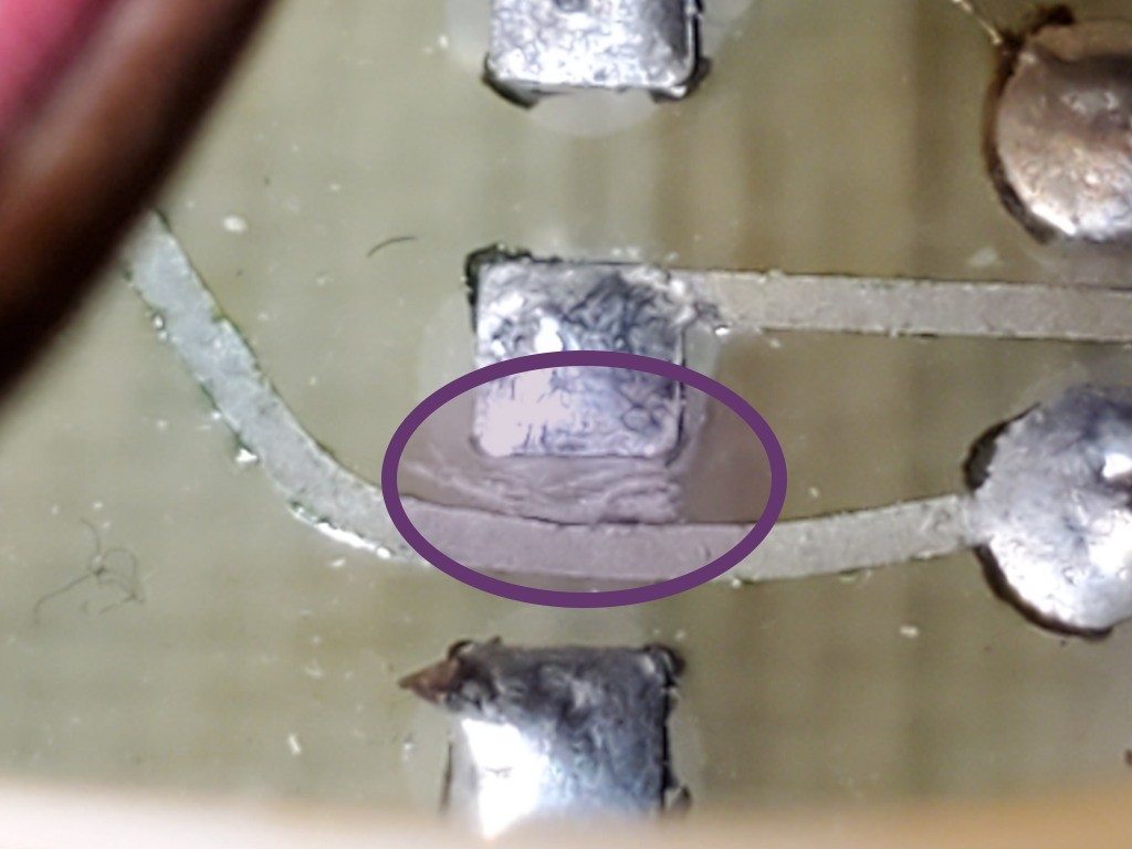
From there, I fetched a bottle of isopropyl alcohol and a wooden toothpick and started scrubbing around the edges of traces while occasionally checking resistance between the trace and ground (the easiest target to stab and a relatively low resistance path to +5V). Using isopropyl by association with cleaning flux, while thinking the choice was really quite arbitrary when I didn't know what there was to dissolve. This was producing no effect -- as expected because I could clearly see that there was nothing there for this exercise to have any effect on. But actually finding nothing would require going all the way around all the edges of all the traces. The unit hadn't been super clean to start with, and there was a little tarnish on the edge connector "fingers". So, onward.
On the back side of the board there was more of some dark something around many of the solder pads. Something like but unlike tarnish or 30-40 year-old flux. Dunno. After a little more scrubbing around trace edges, I scanned around and found a couple of places where the dark whatever around a solder pad encroached on a nearby trace. After a scrubbing at one of those a bit, the resistance between the trace and +5V bumped up to ~100kΩ. Could this be getting at root of trouble at last? After more thoroughly scrubbing out that and a worse-looking spot, the network was isolated. Solved? This time? Really?
I reinstalled Q386, resoldered the cathodes of CR386, CR383, and CR393, and the free end of R386, measured 15kΩ across R386, plugged in the plugin and gave it a try.
It works.
Epilogue
So that's one more 5A26 rehabilitated, and some learning along the way.
Deep breath. For a Dunning-Kruger-powered amateur, that was a tough sprint.
One of the repeating themes of this story has been discovering that I was wrong. That theme continues. Much of this process revolved around a conjecture that Q386 wasn't pulling the gate of Q392 low enough to completely cut off the negative side of channel 2 while displaying channel 1. But maybe that was a red herring all along. I focused on Q392 because I couldn't find any other way for the SWITCH signal to influence the vertical position of the channel 1 trace. And of course what I don't know about must not exist. (And of course I don't like it when other people pull that on me.)
Q386 couldn't pull its collector down because it was drawing current from somewhere other than the resistances in the channel 2 FET switch control. Where was that "somewhere"? The answer to that post-repair question is...
...the source of Q292 (+cathode of CR290+R290+R292) in the negative side of channel 1 that was shifting with the SWITCH signal level. With the fault resolved it's a little hard to check/confirm/refute, but that means that Q392 maybe, or maybe probably, was switching just fine regardless of the less-negative gate drive, like Q382 was. So now it looks like Q386 failing to pull it's collector down into regulation by the zener was just another symptom, a harmlessly inconsequential side-effect, and not causal at all. Maybe.
I think it would be great to hear from anyone who does know what they're doing, and read this, about the face-palm moments where you saw me misread the evidence and pass by more competent options into avoidable digressions.
Thanks for reading my story.