 Electroniclovers123
Last time I DIYed a TA7240 BTL two-channel power amplifier board with 19W power per channel. I wanted to use a transformer for power supply, but the transformer was too expensive and not conducive to mass production, so today I will DIY a switching power supply for it, with 19W for each channel =38W, plus the front power supply, this power supply is designed with 12V5A power of 60W, which is generally enough for application, the design power is too large and the price is not cost-effective. It is good enough for application.
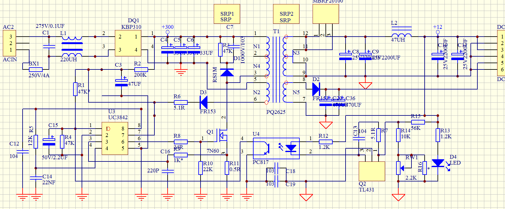
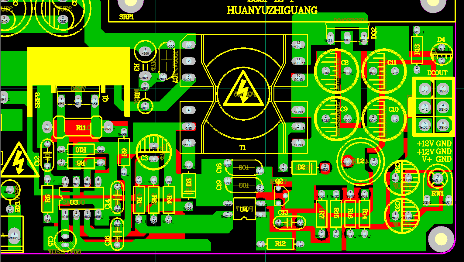
Without further ado, here is the schematic diagram and PCB diagram. Using the classic chip UC3842N, the performance is quite good, the debugging is easy, and the working performance is quite stable.
This is a drawn PCB, which will be sent to proofing tomorrow morning, and will not be proofed if it is too late today.
Wait for the PCB and transformer to come over and then install and test.
After waiting for two days, the PCB proofing finally came back, this is the top-level picture.
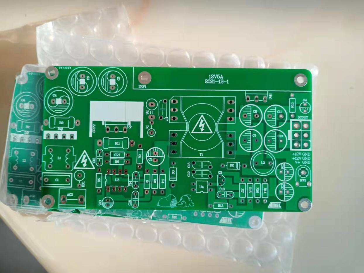
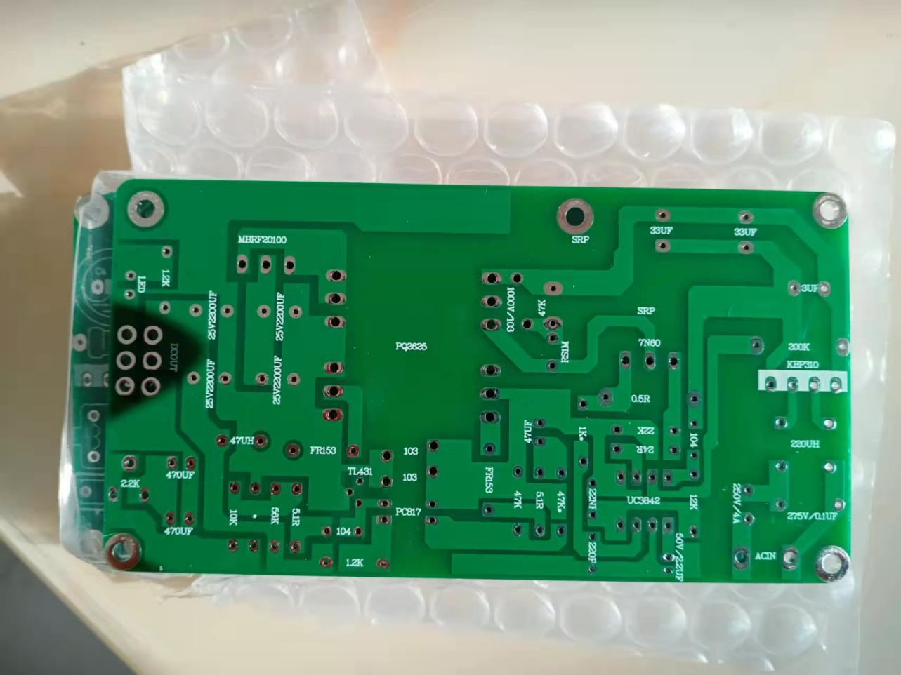
This is the bottom picture. The proofing is back, and the welding board is available for testing. Now the transformer proofing has not come back. Wait for the transformer to be welded.
This is how the components are soldered together. In order to facilitate debugging, a seat is added to the UC3842. The transformer of the PQ2620 is also common to the PQ2625.
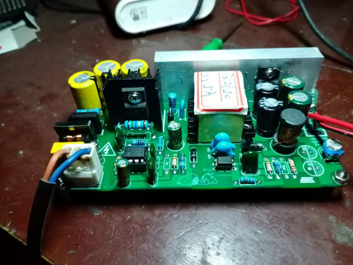
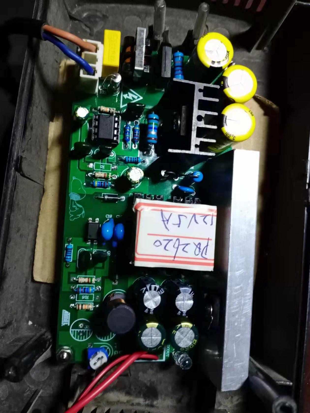
This is what the top looks like. Now that the aging is completed, the parameters are tested normally, and it has little to do with the design. The key is that the ripple control is quite good, almost negligible. No high-frequency noise can be heard in the mute state of the power amplifier.
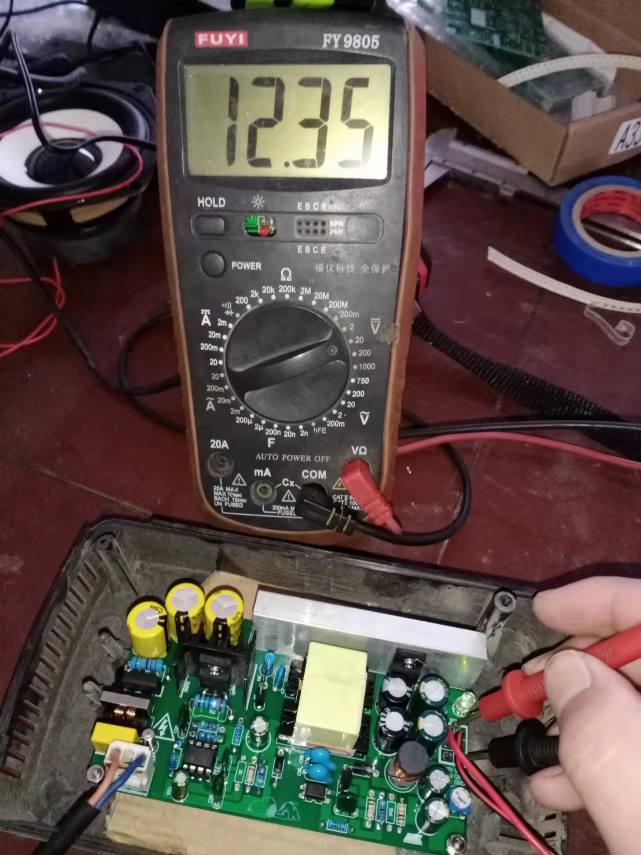
Both no-load and full-load are 12.35V, and the control loop is quite stable. Although it is only for DIY, the design parameters are based on industrial grade, and the materials used are not worse than industrial grade.

 Dave's Dev Lab
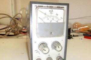

 Krzysztof Wrzalka
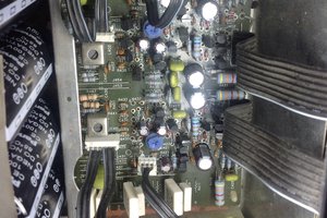
hi, do you sell that pcb? or perhaps you can advice me where I can buy that pcb, many thanks, cheers.