Close
0%
0%

Light Board v2.1

This is a custom PCB we designed in order to control up to six high-power light sources mounted on our rover via CANBus.

Similar projects worth following
319 views
0 followers
This custom PCB was designed in KiCAD for the purpose of controlling the lighting systems on our Mars Rover. Communication with the brains of the rover is done over a CANBus network that we have implemented to communicate with various robotic limbs and peripherals.

The goal of this project was to design a custom PCB that could drive all the lights required to help our rover see in the dark!

Originally, our lighting control was managed by an Arduino soldered to a perf board, and screw terminals were used to connect all the wires out to the lights. 

When we decided to overhaul our electrical systems, we decided a redesign of this component could help reduce maintenance overhead since hooking up dozens of wires to screw terminals can be very monotonous. Additionally, since we had started to implement CAN Bus communication to integrate the rest of the rover's electrical subsystems, such as the steering and drive system, as well as the robotic arm, adding the light system to that list was an easy choice and allows us to use CAN Bus as the central communications hub for all control tasks.

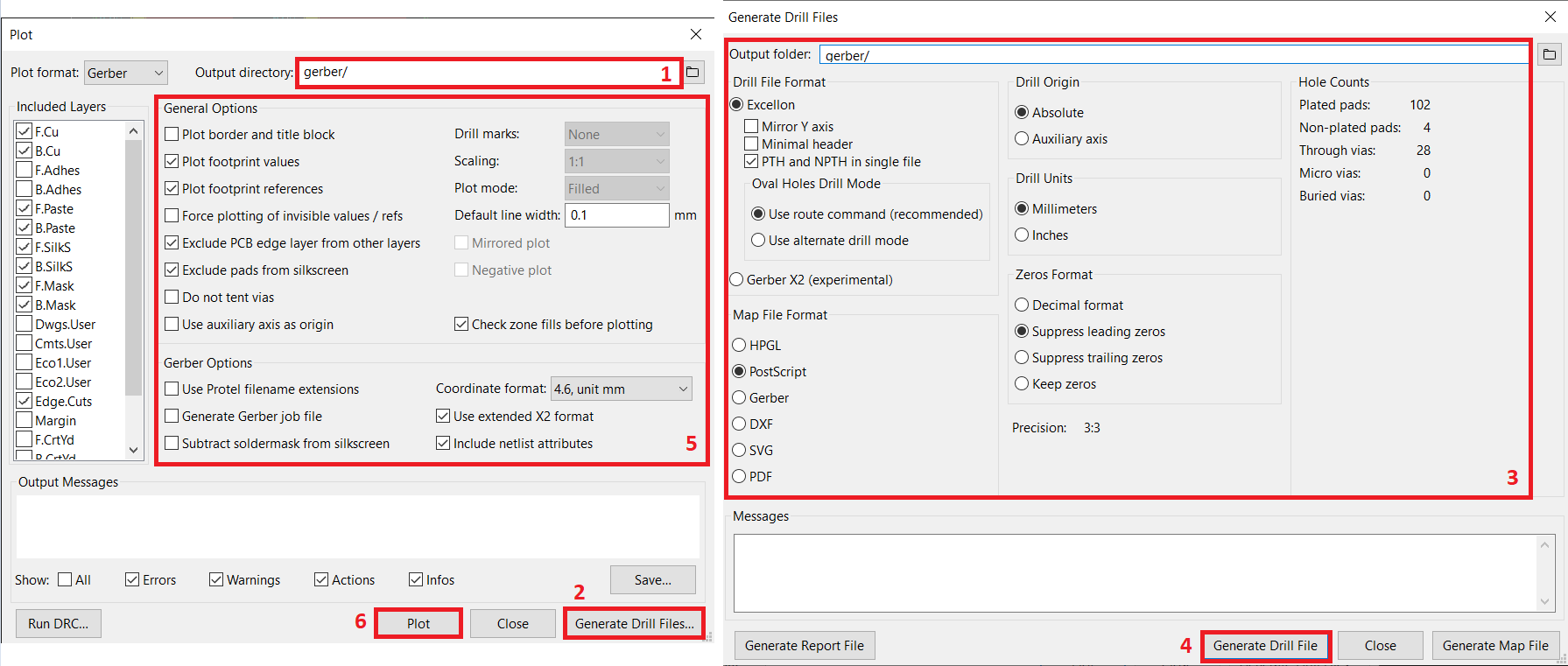
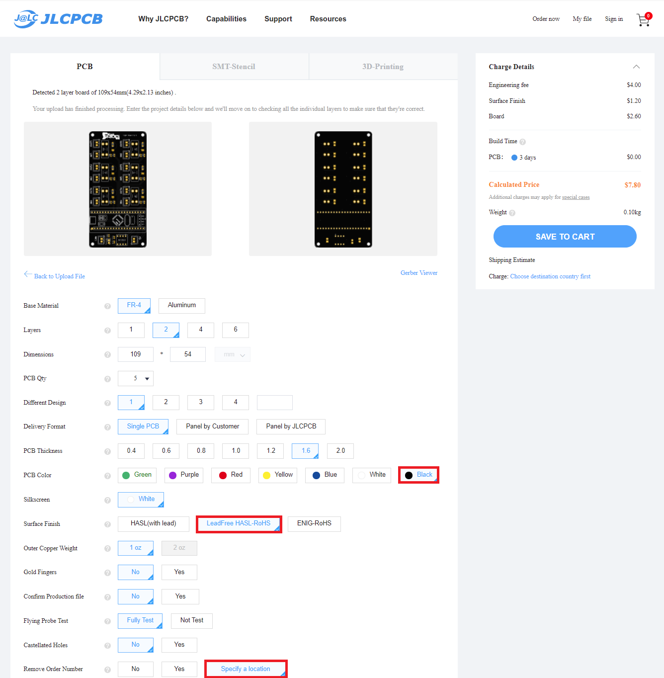
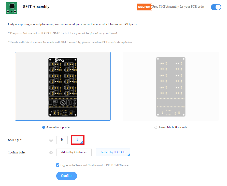
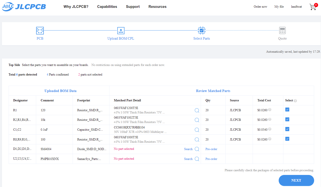
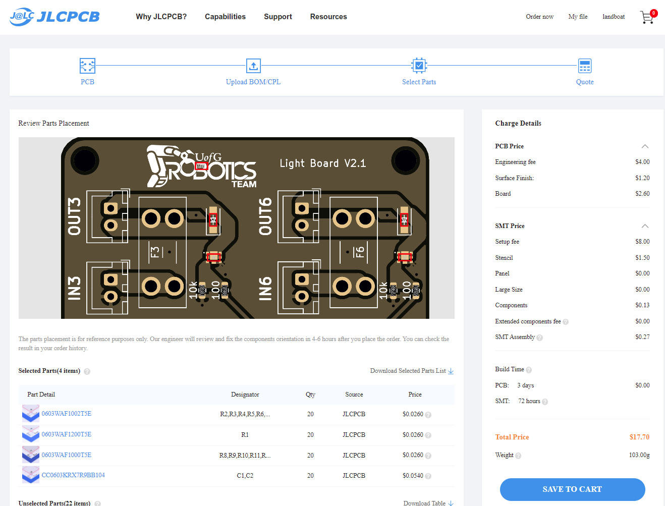
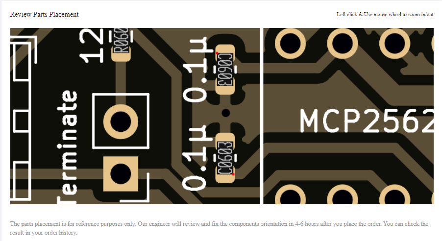
This article will go through some of the engineering design decisions that were made in the development of this board, and will walk through the entire process from schematic capture all the way through to ordering the final product from JLCPCB. 

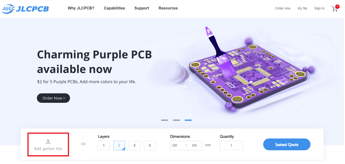
Thanks so much to JLCPCB for sponsoring the fabrication of these boards! JLCPCB provides rapid production of high-quality custom PCBs at very affordable prices, and with the best customer service. If you are looking to fabricate a small or large batch of PCBs for your next project, take a look at the capabilities JLCPCB has to offer!

https://jlcpcb.com/HAR

schematic.pdf

The schematic of the light board PCB

Adobe Portable Document Format - 125.08 kB - 02/24/2022 at 18:22

Preview
Download

  • 1 × Custom PCB from JLCPCB JLCPCB makes high quality custom PCBs at low prices! They offer discounts to new customers too!! https://jlcpcb.com/HAR
  • 1 × STM BluePill (STM32F103C8T6) Microcontroller receives CAN messages and controls PWM to each light output. https://stm32-base.org/boards/STM32F103C8T6-Blue-Pill.html
  • 6 × Fuse Socket Mini Blade type fuse socket. Used to ensure lights operate safely and do now draw more power than expected.
  • 6 × PMPB10XNX N-Channel 30 V 9.5A Surface Mount Power MOSFET
  • 1 × 2.54mm Shunt Used to bridge the CAN network termination pins

View all 13 components

  • Schematic Capture and Component Selection

    UGRT02/24/2022 at 21:16 0 comments

    The first step in any PCB design is creating and validating a circuit. This is a vital step, as fabricating a PCB based on a non-functioning circuit is sure to leave you disappointed!

    Circuit Schematic

    We had validated the 'prototype' of this board with our original rover design, which ran lights from an Arduino outputting PWM signals to control the gate voltage of a power MOSFET. This gate control allows us to take a high-power input from our battery, and control the output voltage so that we can switch on/off and dim the brightness of our LED headlights as needed. 

    We know this control scheme works from our original rover, but Arduino's do not support CAN Bus natively. Rather than try to interface a CAN > SPI interface with our existing Arduino setup, we decided switching to a microcontroller that does support CAN would be worthwhile. We also chose to update a few other components on the board in order to keep its physical footprint as small as possible so as to fit inside the rover's electrical enclosure. 

    Many of the components were chosen fairly arbitrarily; passive components for their cost/availability, and the CAN transceiver, connectors, and fuses/fuse holders simply for consistency with other electrical subsystems. There were a few components that needed to be selected carefully though, and these components were chosen as follows:

    STM BluePill:

    We settled on the popular STM BluePill for several reasons, but mainly because we are already using STM MCUs for several other embedded subsystems, and we have learned that keeping embedded hardware consistent saves a lot of headaches from sourcing and integrating random open source drivers :). It is also small, supports CAN natively, it has ample PWM outputs, and was cheap and widely available before the chip shortage, so hopefully that doesn't last forever!

    Shoutout to yet-another-average-joe on GitHub, who has developed some really nice KiCAD footprints for the BluePill. It is important to use a symbol that matches the exact hardware you will use in any design. This seems obvious; however, we accidentally wired up the symbol for the STMF103 microcontroller itself, rather than the development board first. It can be confusing because although the BluePill houses this MCU chip, the pins on the dev board are not a 1:1 representation of the pins on the IC. 

    Nexperia MOSFET:

    We needed a MOSFET that could drive our LED headlights, but also wanted to build in some tolerance so that we could safely drive higher current loads in the future. Another important consideration was that since this circuit is controlled by a 3.3v GPIO output, we require what's called a 'Logic FET', meaning one whose gate can be driven by 3.3v. There are some drawbacks to these type of FETs, mainly higher Rds values, which basically equates to how much heat they produce. For our application we won't be driving these FETs to their limit, and the benefit to using logic FETs is that a GPIO output can be used to drive the gate without adding extra ICs to the circuit such as a gate driver.

    With these considerations in mind we settled on the Neperia PMPB10XNX, a logic FET with a drive voltage between 1.5-4.5v, and a max Rds ON of 13mOhm @ 9.5A. We won't need anywhere near 9.5A, in fact there are other design aspects that will limit us to driving a maximum of 3A for each light. This limit comes from the JST XH connectors we have chosen. This board needs to be small more than it needs to be capable of driving high current loads, and since the headlights we currently have only actually draw around 1A, 3A is plenty of headroom and 9.5A is honestly a bit ridiculous anyway! We could always remove the JST connectors from a channel if we needed to drive more than 3A; however, in that case, the 2mm trace width on the PCB becomes the next limiting factor, allowing us to drive a maximum of just under 4A. 

    Again, this is just a hypothetical discussion to illustrate the limits of...

    Read more »

View project log

  • 1
    Preparing project for export

    JLCPCB offers custom PCB fabrication and SMT assembly services at https://jlcpcb.com/HAR!

    SMT soldering can be fun, but it requires some special tools, it takes practice to do well, and it can be very frustrating along the way! 

    We decided to use JLCPCB's SMT assembly service for these boards to make things as easy for us as possible. The following steps outline the process to setup your KiCAD project so that you can export all the proper files such as the footprint position (.pos) file, Bill of Materials (BOM), and of course, the all important drill and gerber files.


    Step 1: Creating BOM

    First, you must navigate to Edit Symbol Fields (1) from within KiCAD's schematic window, and add a new field (2) called LCSC Part # (3). Then you just have to add JLCPCB part numbers for each of the components you would like to have assembled for you (4):

    Most of the components on this board are actually through hole (THT) and not surface mount (SMT) since it is mostly connectors. We will have to add these parts once we receive the boards as JLC's assembly service currently only supports SMT devices. That is okay because THT soldering is much easier and faster than SMT soldering and we can still save time by using JLC's SMT assembly for all of the SMT components we need.

    JLC's parts database is simple to use once you know what parts you are looking for. For example, finding the part number for the 0.1uF capacitors above (4), is done by searching for something like 100nF 0603We usually check the Basic parts box as shown below since these are the easiest parts to source, and avoid potential surcharges:

    Once you have input part numbers for all of your SMT components into KiCAD, you are ready to generate a BOM.

    As seen in the screenshot below, start by clicking on the BOM icon in KiCAD's schematic window (1). There is a handy script available to download from arturo182's GitHub that can be added into KiCAD as a plugin (2), which will automatically generate a BOM following the conventions that JLC specifies on their website. Once added, you should be able to click Generate to create the BOM in .csv format (3):

    I personally had issues running the script within KiCAD, but was able to execute the script from the command line. Judging from some comments on the GitHub, this may have been due to spaces within my KiCAD project path, but YMMV.

    With the .csv BOM file generated into your project folder, create a new folder called assembly inside the root project directory and move the BOM file inside this folder. I also like to append a -BOM suffix to this file. This just keeps the project directory better organized.


    Step 2: Generate Footprint Position File

    Next you will need to generate a footprint positions file so that JLC's Pick and Place machine knows what orientation each of your parts need to be placed. This is crucial for polar components like electrolytic capacitors, or integrated circuits, while others like resistors and ceramic capacitors don't matter if they are placed one way or another, so long as they are placed on the pads!

    You must have the KiCAD layout window open to generate this file. Navigate to File > Fabrication Outputs > Footprint Position (.pos) File, then set the Output directory to the assembly folder we just made (1), set the parameters as shown (2), and finally click Generate Position File as seen in the screenshots below:

    To keep the files better organized, I like to rename this file with the suffix -Footprint-Positions rather than -all-pos, just to make the file name more meaningful. You need to open this file and rename the headings to comply with JLC's requirements. The screenshot below shows the proper header names after changing them in Excel:


    Step 3: Generate Gerber Files

    Finally, we are ready to generate the gerber (.gbr) and drill (.drl) files. 

    First, we should create another new folder in the project root called gerber.

    Then, again from the KiCAD layout window, navigate to File > Plot. In the window that appears, set the Output directory to the gerber folder we just made (1), click Generate Drill Files (2), confirm the default drill file parameters (3), click Generate Drill File (4) then close the Generate Drill Files window, confirm the default gerber parameters (5), and finally click Plot (6), as shown in the screenshots below:

    Lastly, you need to zip the contents of the gerber folder into a .zip file before you can move to the next stage of uploading to JLC's website.

  • 2
    Uploading to JLCPCB

    Now comes the fun part! Head over to https://jlcpcb.com/HAR and click on Upload gerber file, as shown below:

    Once uploaded, you can make changes to the default settings applied for your PCB, based on the gerber files. 

    The only things we changed are the PCB colour to black (the new purple colour would undoubtedly look awesome, but unfortunately it is not one of our school colours!), the surface finish to the lead free HASL option, and we have also chosen to specify the order number on the backside of our PCBs by placing the text JLCJLCJLCJLC on the rear silkscreen layer. These changes are indicated in the screenshot below:

    Next, we need to set our parameters for the SMT Assembly service. As seen below, we only chose to assemble 2 of the 5 boards we have ordered. We really only need one of these boards but 5 is the minimum quantity of PCBs you can order, and 2 is the minimum quantity that you can have assembled. There is also an option to specify where the tooling holes will be placed, but we chose to leave this up to the engineers at JLC since this board is not very crowded and we are not picky.

    Next, after uploading both the BOM and footprint placer files, you will reach the following screen where you can verify that the JLCPCB part numbers you entered into KiCAD match the components that will be assembled:

    After verifying the part numbers, you are ready to move on to the next stage of verifying the components' orientations.

  • 3
    Verify component placement

    The last step before you are ready to order your PCBs is checking the orientation of your assembled components. 

    As seen in the screenshot below, the JLC website gives you a preview of your PCB which you can zoom and move around in order to check how it thinks certain parts should be oriented:

    The red boxes indicate components that are not going to be assembled by JLC. In this case, JLC did not have the diode and MOSFET IC that we wanted and so we opted to exclude those components from the assembly. This is done simply by not specifying a JLCPCB part number in the BOM file.

    As for the parts that will be assembled, there are no components for which orientation matters and so there is nothing much for us to check here. This viewer is a good place to do a final check on the placement of pads and traces, and it just so happens that on the right hand side of the image above we noticed that there is a trace that could be too close to the edge! We will go back and fix this before submitting our gerbers for fabrication.

    Although the capacitors we are using are not polar components, the viewer seems to still indicate what would be the positive pad. For illustrative purposes, consider the screenshot below:

    As you can see by the red dots indicated by JLC's viewer tool, if these were polar capacitors, those pads would be where the footprint location file thinks the anode (positive terminal) will be. If this does not match your circuit schematic, you would need to open up the .pos file in the assembly folder, and adjust the Rotation parameters accordingly.

    And that's all there is to it! There are some steps you need to be careful to do properly, but overall JLCPCB makes custom PCB fabrication as straightforward as it could be. And for under $18 CAD they offer incredible value for their services, with fantastic customer service!

    Check them out at https://jlcpcb.com/HAR! They even offer coupons for new users!!

    Thanks JLCPCB for sponsoring our custom PCB fabrication  - we can't wait to work with you again!

View all 3 instructions

Enjoy this project?

Share

Discussions

Similar Projects

Does this project spark your interest?

Become a member to follow this project and never miss any updates