 kelvinA
[20:00]
So I've continued processing changes for Tetrinsic and #Tetent [gd0090], but am trying to focus on Tetrinsic for now since it's what holding back progress. My main concerns have been written in this log.
Today, I've been trying to figure out how the mcu is flashed. Apparenlty, it's via an "Nu-Link" device. I can only assume there's some kind of bootloader already on the chip so that it knows which pins are the ICE pins.
Then I was wondering how I was going to set the device addresses for I2C.
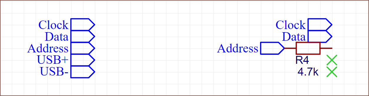 The 5 pin ribbon cable looks like this right now. There's not really much space, so I've put the USB data lines on it too and plan to not have a connection for the cable that goes to the next Tetrinsic. This way, only one Tetrinsic in a chain will have a USB connection, and this one will be the master Tetrinsic.
 For addressing, my plan was to have a way to detect the resistance value between the Sense (now called Address) line and some other line, but I don't think my idea would work when there's more than 1 Tetrinsic on the lines.
Instead, I've got another idea where
- The end-Tetrinsic sends 3.3V down the Address line (via soldered pad on board)
- The Master Tetrinsic connects the line to ground (via soldered pad on board)
- If the voltage measured on the Address pin = 0, this is the Master Tetrinsic and it uses a software defined I2C address. All others will instead opt for a dummy address.
- The voltage measured on the Address pin will determine the delay before trying to connect to the Master Tetrinsic. The master Tetrinsic will give the slave Tetrinsic an address and will log that it was the n-th Tetrinsic in the chain.
In my research, I heard that there was some SMBus thing that had a feature that actually sorted out the device addresses so that there aren't conflicts, but it seems that it's only a feature in the M032xG/I chips and the USCI found in the M032TD doesn't have that feature according to my skim reading.
Oh, and me a few hours ago:
- Man. There's got to be some more information, like on programming the mcu or even some more I2C knowledge...
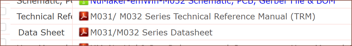
- Hm? What's a TRM? I didn't see this on the specific M032 documents page. It was just the Datasheet and nothing else.
![]()
Opens it
![]()
My face:
![]()


Now I'm really wondering just how much scope this project is going to grow into! The good news though is that I guessed correctly on what pins the USCI uses for I2C. At least Me In The Recent Past got the additional content he desired when saying that the 288 page doc wasn't detailed enough.
Anyway, I looked at the pins and the SPI pins take up some of the ADC pins, and I need an ADC pin for the Address signal.
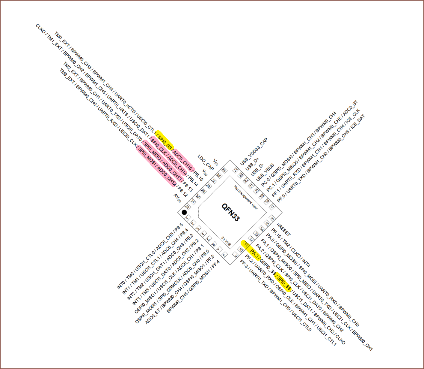 Conviniently enough, there is another set of SPI0_x pins on the other side of the chip, and I'm not using Pin11 (PA.3). Therefore, I've crammed in the traces at the bottom of the board. I haven't imported the new outline yet.
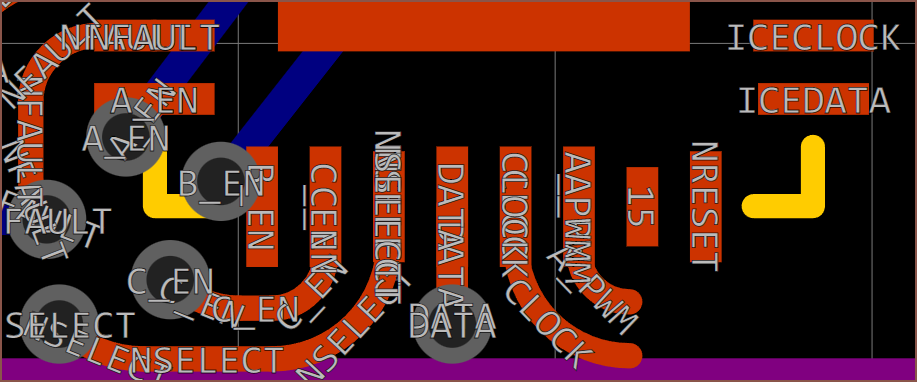 I'm also going to use nReset since this is the first time I'm making a microcontroller board and I don't really want to risk adding any hurdles that could've been avoided.
Since I had the space, I've added a 1u bypass capacitor.
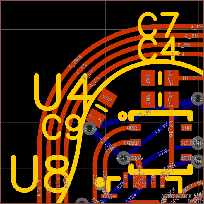 I've also made all the silkscreen text bigger, as I still have to keep in mind the actual scale of this board.
Discussions
Become a Hackaday.io Member
Create an account to leave a comment. Already have an account? Log In.
I just found some good educational content on making custom keyboard microcontroller designs:
https://wiki.ai03.com/books/pcb-design/page/microcontroller-design
https://wiki.ai03.com/books/pcb-design/page/pcb-guide-part-3---creating-the-mcu-schematic
Are you sure? yes | no