 Dimitar
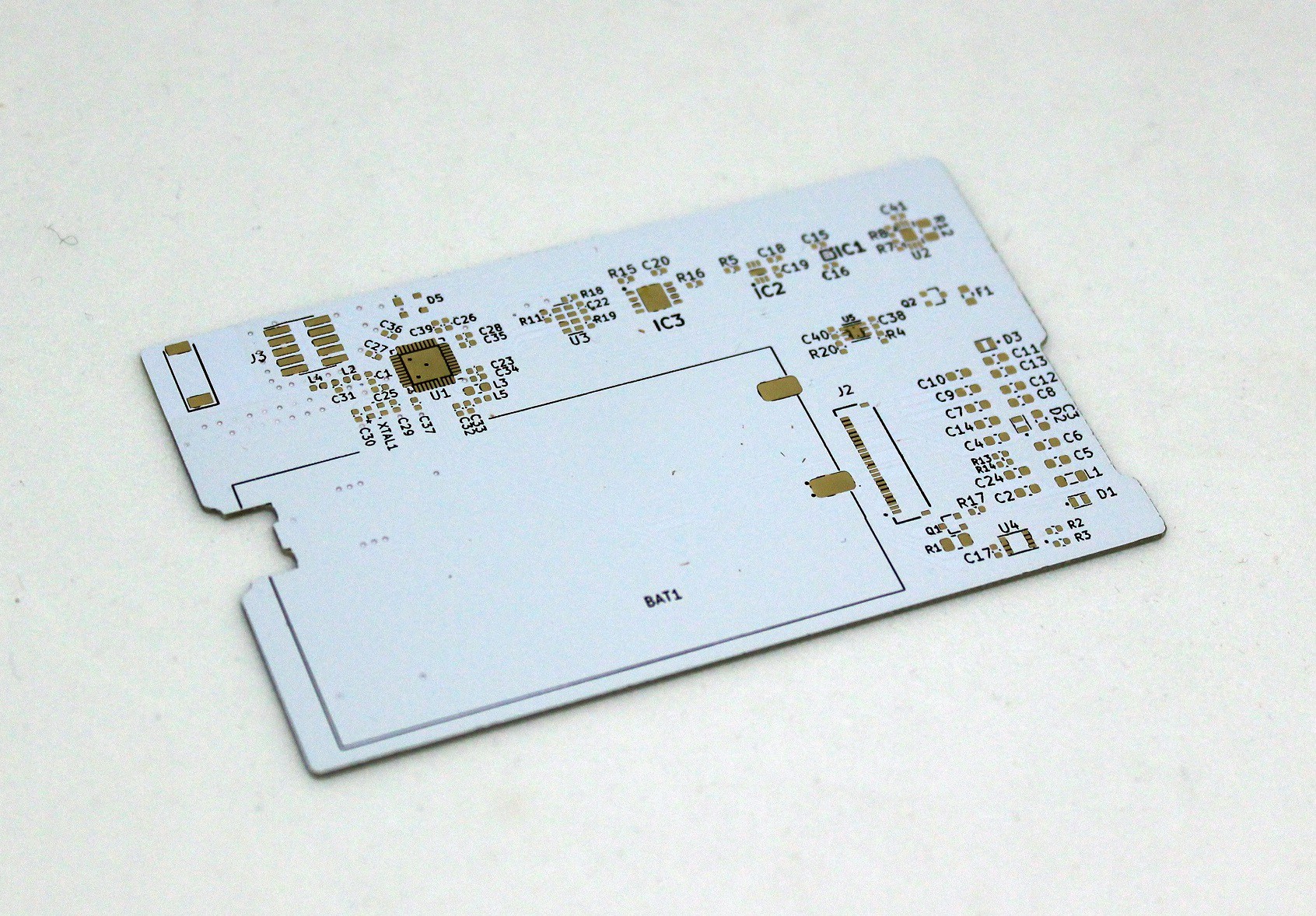
This is the first version of the PCB. I put up the extra money to make it white. I figured it would look more like paper. It didn't. It all went down hill for the white PCB.
The white solder mask seems to come off very easily. You can see it on all fine pitch components. For example the flat flex connector footprint.
I did not make a big deal of it at first. But when the soldering stared. I got a lot of solder bridges. This meant putting a lot of flux.
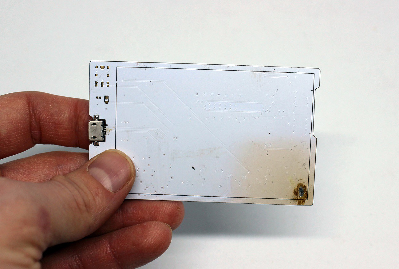
Which brings me to the next point. Every little stain on the board is super visible. At one point it drove me crazy. I had to soak everything in alcohol to clean it.
But wait, there is more. If you over heat the white solder mask (may be you had a lot of solder bridges to fix), it kind of turns yellow / brownish. The effect is done with the help of my hot plate @ 250C. To be honest I did let it on the heat a bit more. But this could easily be done with hot air. So now you know.
May be the green board also change color but it is not so obvious. What ever lets move on.
Next thing I started to add components. First was the LDO. To test it I put two wires where the battery would have been and powered it using my bench power supply. I had 3.3V - perfect.
Next I installed the MCU with all of its bells and whistles. I could connected to it with the debugger and run some code. Yeah baby!
The QSPI flash (SPI in my case) and the RTC were next. Both work from the first time.
Next on the list was the charger. I copy the exact circuitry from the eval board and was not surprised that it was okay also.
At that point I ran out of luck. I tested the e-paper display and it did not work. Sh*t... The radio part of the build failed too. Double sh*t.
It was very important to fined out what was wrong with the board and fix everything before I spend money for revision 2.0
Lets start with the radio part which was surprisingly the easier of the two.
The first thing I thought was the problem, was the low frequency crystal. It was marked optional on the provided examples. Soo I deleted it. It turns out that, it is a really good idea to have one if you had BT, but not crucial. I configured the MCU to use the internal RC oscillator for the radio. Still no bueno.
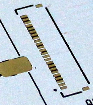
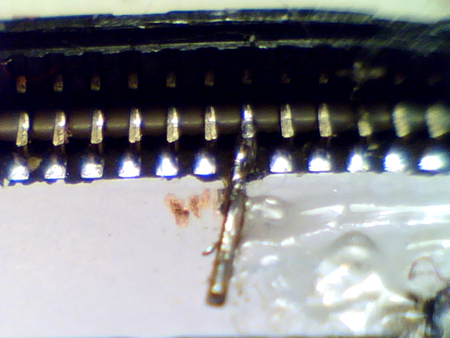
The problem was more annoying. I used the impedance calculator from my PCB manufacturer. This calculator was waaaay off. The track in the picture above is just too narrow. I made some research and found how to calculate it. We are so spoiled with all the tools we have. I will do my own homework from now on.
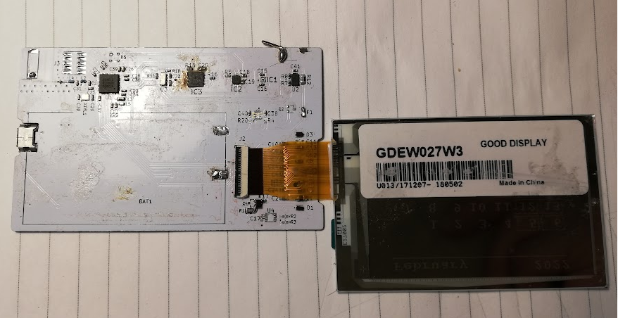
Next was the display.
I have changed a number of components from the example schematic in the datasheet. No surprise there.
- First thing wrong was that number 1 pin on the display was not number 1 on the connector. I took my microscope and looked inside the flat flex connector. It had pins on the top and bottom. So just turn the display around and connected it.
But still no image. I thought I have burn the display. I put it on the Pi HAT and it ran. Lucky for me, that was not the only mistake I have made.
- Looking back at the schematic I have forgot to connect the GND pin. To paraphrase the title of the post. A superior engineer uses his superior design skills, so he does not have to use his superior soldering skills. Unfortunately I don't have superior design skills and had to use my dodgy soldering skills to fix this. I scrape the solder mask (that was super easy as we know already) to expose the GND plane and with a small wire I connected the pin to ground.
Connected everything everything up and nothing. No image. Spicy!
At this point I figured I have made bad selections for my components. Again I got my trusty Pi HAT and desoldered the inductor. Then put the inductor I have chosen on it. It ran. Good. Then I put the diodes I have chosen. It ran again. Excellent. Then the last component was a transistor. And again everything was okay.... wtf.
- I got back to the schematic. Everything was wired correctly. But the footprint for the transistor was not the right one. Again my dodgy soldering skills come into play.
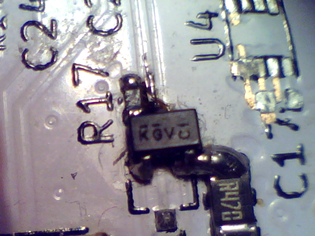
I flipped the transistor. And you guessed it... no image.
Naah I am joking, we got an image ladies and gentlemen. But the display was on the wrong side and the image was flipped.
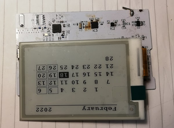
Great everything was working, but if I gave this to anybody they would not be very impressed. Even worse they thing I was mad. Not so great business card so far.
I had to do some more work in KiCAD.
Thank you for sticking till the end. Hope it was fun. There will be more updates to come.
Cheers!
Mitko
Discussions
Become a Hackaday.io Member
Create an account to leave a comment. Already have an account? Log In.