 Arshmah Shahkar
Working:
To understand the working of the SMPS PCB board I have divided the major parts of the circuit board into some blocks which are explained below;
A- Protection from high voltages
B- AC to DC converter
C- Input Filter
D- Diode Clamp circuit
E- Auto-restart mode of power supply
F- EMI filter
G- Rectifier and Ripples reducer
H- LC filter
I- High voltages to low voltages
J- Safety barrier
K- High switching frequency
L- Shunt regulator
M- AC to DC isolation
Design files:
I have designed this PCB board on Altium then I have uploaded the schematic file online on Inventhub for the users who want to implement my design they can view or download it from the given link.
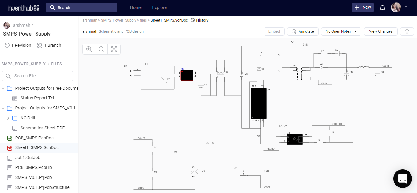
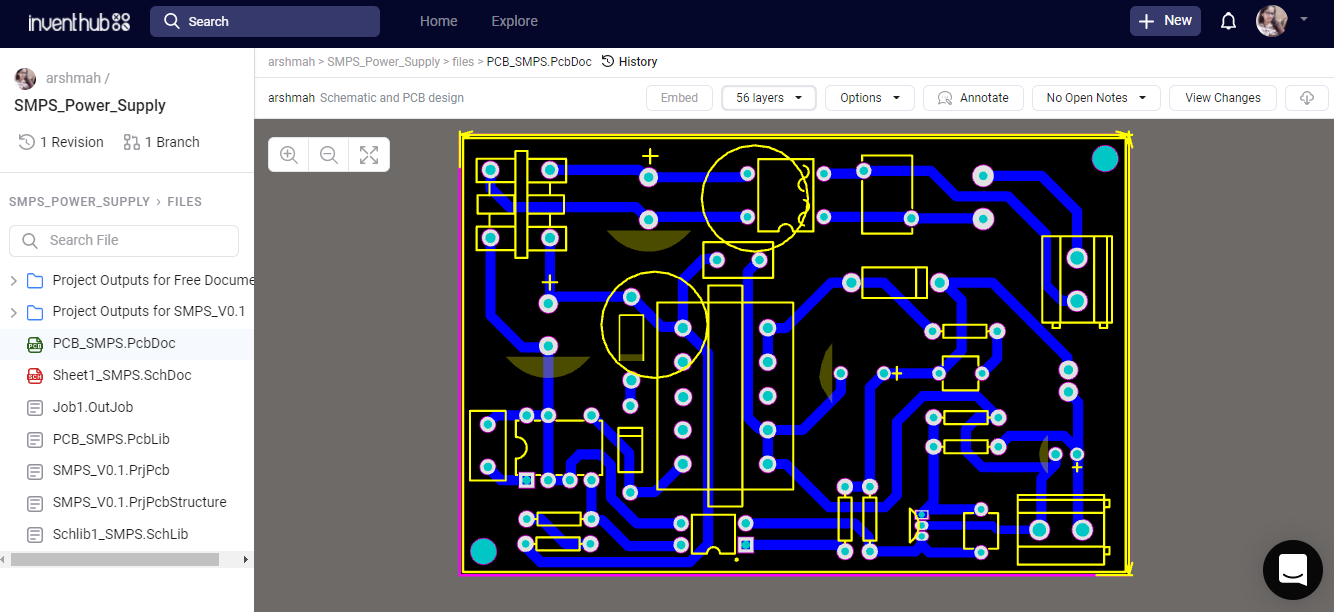
After the implementation of the schematic, I have converted my design to a PCB file so that I can design my board and can view it in 3D view. For the fabrication of my board, I have uploaded my PCB and all design files on Inventhub for the manufacturers. They only need to download the ZIP file format and they can fabricate my PCB board without making any error in the design.
Project History:
I have created multiple revisions in my project and I have uploaded them all online on Inventhub to keep them as my backup design. If I want to use my previous design as my current design I do not need to Undo my current design I can easily use my specific revision of the design by going into my project revisions. I can download and can reuse it as my final design.
BOM file:
I have created a BOM file for those who want to work on my design they want to know about each component and for the component providers to deliver the components. It contains the detail of each component used like dimensions, manufacturer, quantity symbol, and footprint library reference.
 Amar Potdar
 Fabian Butkovich
 Christian Lerche
 miguelmurca