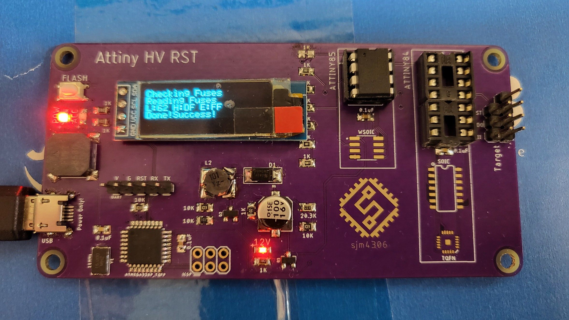
• Design Flaws

    sjm430604/14/2022 at 15:13 0 comments

    So in total it's taken me around 3 months from inception of this project to having a working prototype in my hands. There were a number of problems I encountered, which isn't anything uncommon in my projects lol. It wouldn't be nearly as fun if everything just worked perfectly the first time!

    The first big issue was I flipped the OLED header connection upside down and ended up blowing a screen. Oops, a silly mistake I should have double checked before sending gerbers and definitely before powering on. Fixed in new board files, but for this prototype I just used wires to flip the display the right way around.

    Secondly, I designed the closed loop boost converter on breadboard and then transferred the design to surface mount components on the final pcb. I rummaged through my parts bins for inductors, diodes, capacitors and mosfets I could use. I figured that since the 12V is really only used to trigger the attiny high voltage programming mode and not to power any heavy load so I could get away with pretty small components with low power ratings. The issue I ran into is a bug in the first iteration of my pid software would occasionally shoot the output on full blast, basically shorting the inductor to ground, creating a large shoot through current that the tiny mosfet couldn't handle. This resulted in the first mosfet I soldered releasing it's magic smoke in the first round of tests. This wasn't an issue when I tested with the larger/beefier components on breadboard. I ended up printing out the variables on the OLED in real time, and monitoring them while powering from an external current limited supply. I decreased the gains a bit and decreased the output limiter so I wouldn't set pwm above around 90%. This will affect transient response to heavier loads but for the light load conditions of this design it's not an issue. Since this fix I haven't observed this issue.

    Next, I saw an issue where sometimes the slave chip under programming would sometimes be recognized but sometimes not (causing the whole device to hang). Rule 1 of debugging though shalt measure voltages! The reference circuit I based my design off of used 1K resistors on all pins connected to the slave chip. In theory this looks like a good idea to protect the rest of the onboard circuitry, just in case the slave chip is plugged in backwards or is damaged. The issue is my vcc rail is 5V but the measured slave chip's vcc was only around 2.5V due to the series resistor dropping the voltage when current was drawn through it. My quick fix was just to short that resistor out, and now it works perfectly. I'll probably just end up swapping in a low value resistor in the future, so there's something to limit current but at the same time not drop the voltage so much the chip cant be recognized.

    The final issue was also pretty simple. I was able to detect and program attiny85 chips but not attiny84's! However during one test with an 84 I was able to get it to detect and program! The thing I noticed was that during the test I was touching the board, pressing down on the chip to make sure it was fully seated into the socket. I could not reproduce this however. So I had a feeling it was something related to capacitance or grounding. Reading the datasheet and doing a little google search showed that I had forgotten to ground pins PA0-PA2, which allows the chip to go into high voltage programming mode. Oops once again! I was able to bodge a wire onto the dip pads and get it to work in the end, but the pads for the surface mount footprints are gonna be difficult to bodge so for this first prototype I'll have to use an external smd to dip adapter to flash smaller attiny84 chips. I've already fixed this flaw in the new pcb files.

    So there, I've had tons of fun hunting down these problems (at the cost of some destroyed components and some time) but I had some good 'aha!' moments learning from my mistakes so it's not a waste to me.

  • Theory of Operation

    sjm430604/14/2022 at 14:38 0 comments

    In my recent projects moving to the Attiny series of microcontrollers, I've found a need to be able to reset chips I've accidentally "bricked" through incorrect fuse settings that prevent low voltage serial programming. So in this video we take a look at a pcb I designed based on work by Paul W (https://www.rickety.us/2010/03/arduin...) and Jeff Keyzer (https://mightyohm.com/blog/2008/09/ar...). Huge thanks to Paul and Jeff for their software and hardware which this project wouldn't be possible without.

    So the design is fairly straight forward, it's basically just an onboard atmega328p that is programmed to bitbang the serial programming protocol for reading/writing fuses to the attiny series of chips. The gotcha is to reset fuses for chips that have had serial programming disabled or the reset pin set as a gpio you need to place the chip into a high voltage programming mode. This is achieved by pulling the reset pin high with 12V instead of the normal method of pulling it to ground from vcc. So in addition to the atmega we also need a 12v supply (well technically 11.5-12.5V will do according to the datasheet).

    I can do this easily by powering the whole circuit from a 12V DC wallwart and use a cheap linear regulator to generate 5V for the logic but it's a bit inconvenient to need a separate supply adapter. So I opted to generate the 12V onboard from the USB power input jack. There are quite a few ways to accomplish this but I wanted to try my hand a closed look compensator design. I could've gone with a switched cap converter but in the end I designed a boost converter around discrete components. Controlling these components is the same atmega that's doing all the serial control of the slave attiny chip. I accomplish this by using a timer interrupt to calculate the PID output at a 2kHz sample/computation rate. PWM frequency is selected to be as fast as possible to decrease required component size, and with the atmega this comes to around 32kHz at 8 bit resolution.

    PID calculation in the interrupt is fairly simple/conventional:

    //executes at 2kHz via interrupt, execution takes ~140uS, all voltages in mV
      
      ADCSRA |= (1<<ADSC); //start conversion
      while((ADCSRA>>ADSC)&0b1){;}  //wait till conversion done
    
      //measurement=supply*fbgain*((double) analogRead(FB)/1024);  //in mV
      //precalculate mult=supply*fbgain/1024 to speed up calculation
      measurement=mult*ADC; //grab 10 bit measurement
    
      //Max voltage on reset pin is 13V
      if(measurement>13000){   //safety net, cut pwm if voltage rises above 13V
        OCR1A=0;
      }
      
      error=reference-measurement;  //calculate error and I,D terms
      integral+=error;
      derivative=error-last_error;
      
      if(integral>limit){integral=limit;}    //set term limits to prevent excessive windup
      if(integral<-limit){integral=-limit;}
      
      if(derivative>limit){derivative=limit;}
      if(derivative<-limit){derivative=-limit;}
    
      output=p_gain*error+i_gain*integral+d_gain*derivative;
    
      if(output>240){output=240;} //limit output within pwm control range
      if(output<0){output=0;}
    
      OCR1A=output;  //set pwm value to calculated output
      last_error=error;  //update last error value

    The analog voltage at the 12V rail must be measured by the atmega, this is handled by using a voltage divider (iirc I used 10K and ~20K resistors to safetly drop the output by a gain of ~0.3, within the 0-5V range of the atmega ADC). The software multiplies by the inverse of this gain in order to calculate the unscaled original voltage.

     This compensator runs continuously shortly after power is plugged in and will constantly adjust the boost converter output to 12V. There is an additional transistor on the 12V output which allows the atmega to set the attiny's reset pin to either 12V or 0V.

    When the start button is pressed the atmega reads the device identifier for the chip to determine what slave chip is attached and thus can look up the correct fuse settings. It will then read the current fuse values, program the new ones and then read back the values...

    Read more »

  • Demo Video

    sjm430604/14/2022 at 14:06 0 comments