Phil Wright
-
Register File Deux
11/28/2016 at 00:09 • 13 commentsThanks to Yann Guidon for pointing out how the design of the register file could be improved in order to save on components. In fact the previous design used a total of 255 IC's over 45 PCB's. Based on the feedback I have come up with another design that brings the number down to 138 IC's and 18 PCB's. Quite the saving!
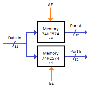
The Register Store design has been changed to remove the use of separate output buffers and instead uses the built in output buffering capability of the 74HC574 IC. In order to make that work we need to store the value twice, once per output port and then use an incoming enable line in order to control when the value is output. Although crowded, we can fit the 8 x 74HC574 and all the headers onto a single board and so reduce the number of PCB's by half as well as saving on IC's. The block diagram is very simple...
![]()
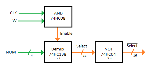
We used to have a Register Select for each register. But instead of providing the register numbers to each register we can use a de-multiplexer to convert the binary numbers into selection control lines that are then distributed to each storage board. That means we have the selection logic once rather than for every register. Here is the block diagram for dealing with the register write functionality...![]()
The NUM is just a 4 bit binary number that comes from the instruction and is the target register to be written to. But we only want to write when the CLK occurs and the W (write) control line is high. Instruction decode logic elsewhere will decide if the W should be high based on the specific needs of the instruction. We need 2 x 74HC138 IC's to perform the de-multiplexing resulting in 16 output select lines. Because the 74HC574 memory IC needs an active low signal for writing a new value we need to invert all 16 lines before distribution.
Two more copies of this board are needed in order to generate the port A and port B output signals based on values from other parts of the current instruction. They are simpler in that they do not care about the CLK and W signals, they always output something on both ports at all times. To keep costs down I will use the same design for all three boards but the port A and B instances will have jumpers that connect the CLK and W to high so that the output is always applied.
I should be able to get this designed in Eagle during the next couple of days and then ordered.
-
Register File
11/25/2016 at 00:20 • 3 commentsYou can see the specification for the user level RISC-V ISA by going to the http://riscv.org website and looking inside the specifications menu section. We are going to be implementing the RV32E specification. This is a 32 bit machine with the embedded microprocessor (E) extension. It only requires 16 general purpose registers instead of the standard 32 and it also makes optional some of the features that would otherwise be mandatory.
Our first design step is to work on the register file as it is the heart of the processor. It needs to need the following requirements...
- 32 bits per register
- One input port
- Optional write per cycle
- Two output ports working in parallel
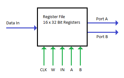
Here is out black box diagram for it...
![]()
The blue input port (Data In) and output ports (A and B) are both 32 bit buses. The green control lines provide a clock signal (CLK) and a write (W) line. Only if the write line is high does a target register get updated on the clock signal. Most processor instructions do not cause a register to be updated so the W line will only be high for update instructions. The IN control line is 5 bits wide and specifies the target register for the write. The A and B control lines are also 5 bits wide and identify the register to output to the matching port. Five bits gives us 2^5 = 32 possible target registers. Strictly speaking we only need 4 bits to encode the 16 registers but I went with the 5 for a couple of reasons.The RISC-V instructions have 5 bits assigned to selecting registers and so it becomes natural to pass those instruction bits straight to the register control lines without throwing one away. Plus, in the future it would be easy to expand the processor to have the full 32 registers if I decide to switch from the RV32E to the RV32I specification. It is easy to make it 5 instead of 4 at this stage and we might as well leave future options open by doing so.
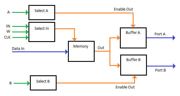
If we expand into a high level design we get the following...
![]()
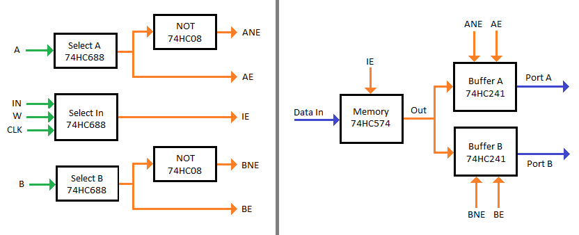
To implement the output ports we need to ensure that only 1 of the possible 16 registers outputs to each port at a time. So we use buffer drivers on each port. In order to decide if the buffer should output or be high impedance we use the selection logic on the left side of the diagram. They do a compare against the A and B control lines to decide if this register is selected. To update the memory we need to ensure we are the selected IN register along with the write line being high and the clock high. Only if all three constraints occur should the memory update occur.Converting this into an actual logic chip design we get...
![]()
First you will notice we have split the register into two half's, the left side is performing the selection logic and then the right half is implementing the actual memory and output. This is because there are too many logic chips to fit on a single 100mm x 80mm PCB if it was all implemented at once. So we are forced to split it into more than one board. You will also note that the output buffers suddenly have two control lines going into them.The 74HC241 buffer driver IC has an odd specification. It has 8 input lines and 8 output lines but they are split into two blocks of 4. The first block output on a high enable value but the second block outputs on a low enable value. So to get all 8 lines to output (or to turn the output off) I need to provide two control lines that are inverted from each other. Hence on the left side of the diagram you will see there are two NOT gates used to provide those inverted values.
Register SelectThe left side of the diagram will be implemented as the Register Select board and contain the following components...
- 3 x 74HC688
- 1 x 74HC08
- 4 x 100nF bypass capacitors
- 1 x 5 position DIP switch
- 5 x 4.7k ohm resistors
- 3 x LED
- 3 x 470 ohm resistors
- 2 x 10P long female headers
- 1 x 8P right angle female header
Each board will have a DIP switch that is used to define the register number along with 5 pull down resistors for when the switch is in the off position. There are three LED's that indicate the value of the IE, AE and BE output lines. That will help with debugging by allowing us to quickly visually check the results of the board.
To provide the incoming control lines we use two long female headers. One of them will have the port select A and B and the other all the other controls lines. Using long female headers means we can act stack all 16 registers on top of each other (Arduino Shield style). The right angle header carries the outputs to the Register Store board.
I have already created a prototype board, it looks like this...
![]()
Register Store
The right side of the diagram will be implemented as the Register Store and contain the following...
- 2 x 74HC574
- 4 x 74HC241
- 6 x 100nF bypass capacitors
- 3 x 16P long female headers
- 3 x 8P right angle female header
- 1 x 8P right angle male header
No doubt you will have noticed already that this only handles 16 bits and not the full 32. There is not enough room on a 100mm x 80mm to fit the 12 IC's needed to fully implement a 32 bit register. That would be 4 x 8 bit memory chips and 8 x 8 bit buffer drivers. When you add in the 32 incoming data lines and 64 output lines needing headers then it becomes impossible. So instead the board implements exactly half the storage. Then we can daisy chain two of them together to get the full 32 bit wide register.
A right angle male header brings in the control lines in from the Register Select board. A right angle female header on the opposite side of the board sends it out again to the next daisy chained Register Store board. It has three long female headers that bring in 16 data lines and sends out 2 x 16 port lines. Finally there are two right angle female headers that always give the current memory contents output. This is not shown on the design diagram and will be used to help with debugging. By attaching an external board that shows the current value it will be possible to monitor what is happening when single stepping the CPU.
I have created a prototype of this board as well but do not currently have a picture, I will add it later.
Both the boards had small errors that require them to be corrected and remade. I aim to order them in the next week and have them ready for testing at the start of December. I will update with the results when that happens.
-
Eagle and PCB
11/23/2016 at 04:59 • 0 commentsThe finished design is going to be quite big. It has to implement the 40 odd instructions of the RISC-V user level ISA as well as handle all the 32 bit data/address buses and connections. So creating it as a big breadboard project is out the window. No. We need to create some actual proper PCB designs that can then be connected together in a modular fashion.
So we need to use software to design the PCB and then have them manufactured. As a hobby project this needs to be a cheap service. So I have decided to use Eagle. If we stick to just 100mm x 80mm boards then the software is free. So that places a constraint on the maximum size on any of the boards we make. Looking at manufacturers I found a Chinese company called PCBWay that seems about the cheapest option. They can provide 100mm x 100mm boards at just $10 for 10 of them. Even when you factor in postage at $25 that is still only $35 for 10 boards of a professional quality. This is the cheapest way I can find and fits in with the hobby cost I can afford.
So all the components that make up the CPU need to be built from 100x80 PCB boards that can then be connected together using either simple ribbon cables or headers that directly plug together. In fact, this sounds ideal as each board can be designed and iterated quite cheaply until it works perfectly. All whilst keeping the cost down to a manageable level.
World's first 32bit Homebrew CPU
Creating the world's first 32bit homebrew CPU using 74' series logic.