Time-lapse:
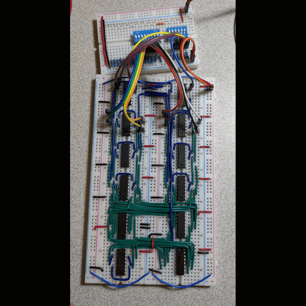
Table of contents:
- Summary
- CPU
- RAM
- VGA
- Keyboard
- Power Delivery
- Components
1. Summary
This project is a physical implementation of the Hack Computer, as described in the From Nand To Tetris course. The course describes the hardware design of a simple computer and the software stack on top of it. The computer described in nand2tetris makes some assumptions on the behavior of the Memory and I/O so I had to design and implement these components in a way that works with those hardware assumptions. I implemented the design on breadboards using mostly 74-series ICs and wires that I cut and connected between the ICs.
I took the nand2tetris course in my 4th year of my Electrical Engineering studies and during the course wondered if the Hack design can be physically implemented. I searched online and saw that the Hack computer was implemented on a FPGA, but I thought it would be so cool to see it running on actual chips and decided to go for it. I first thought about the idea of using only NAND gates, as we did at the actual course, but quickly understood it not feasible to do so. I decided on using ICs of basic logic elements like logic gates, MUXs, Adders and Counters.
Now, after about 2 years, I finished building the computer and it works perfectly. I had many challenges along the way, some with the design work and some with the implementation work. I needed to design the VGA and Keyboard controllers from scratch, and adjust the design of the CPU to work with a physical RAM chips. I also had bugs, so many bugs. Some bugs were design issues and oversights, and many of them were due to physical and analog phenomena that occurred on the breadboards. I had no idea when starting this project that I will need to invest that much time in fixing issues with signal noise, power delivery, reset and clocks. Also, the debug work got harder and harder the more components I added to the breadboard so I had to build tools for debug as well.
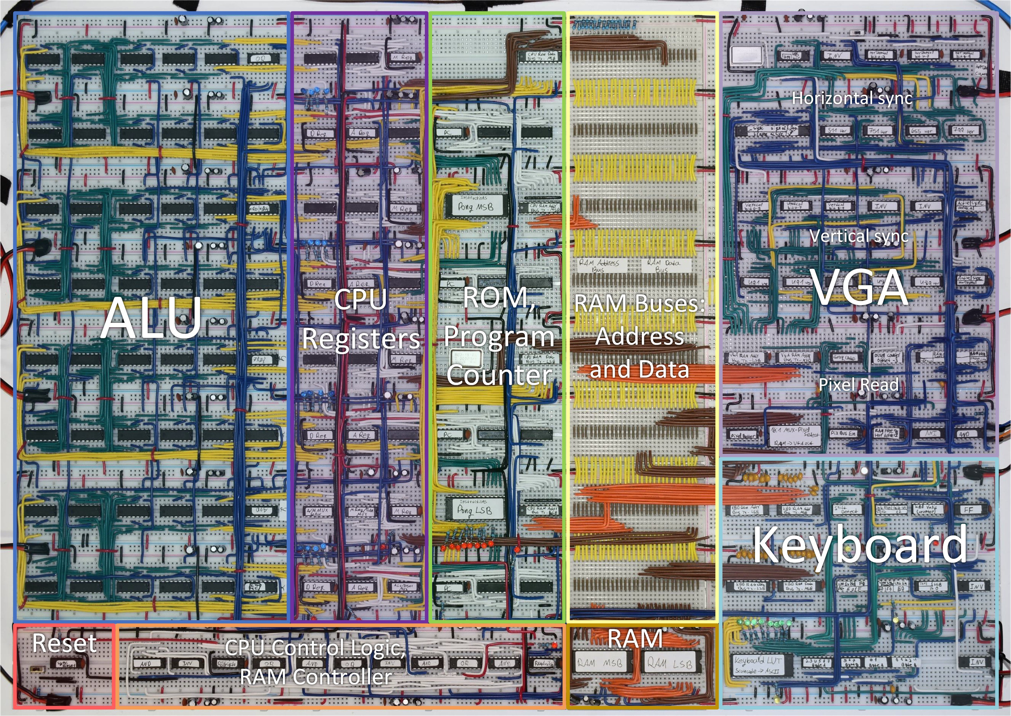
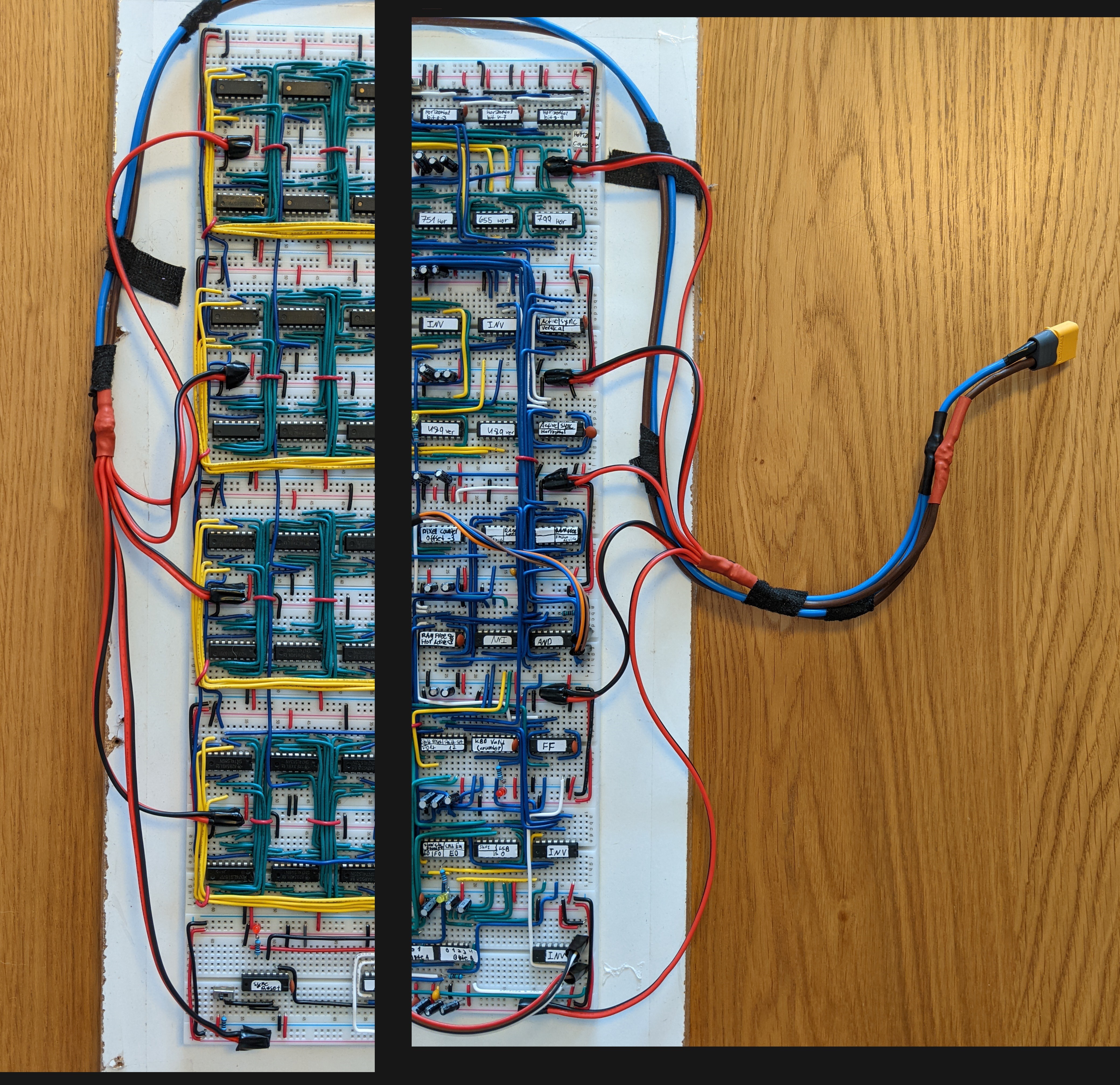
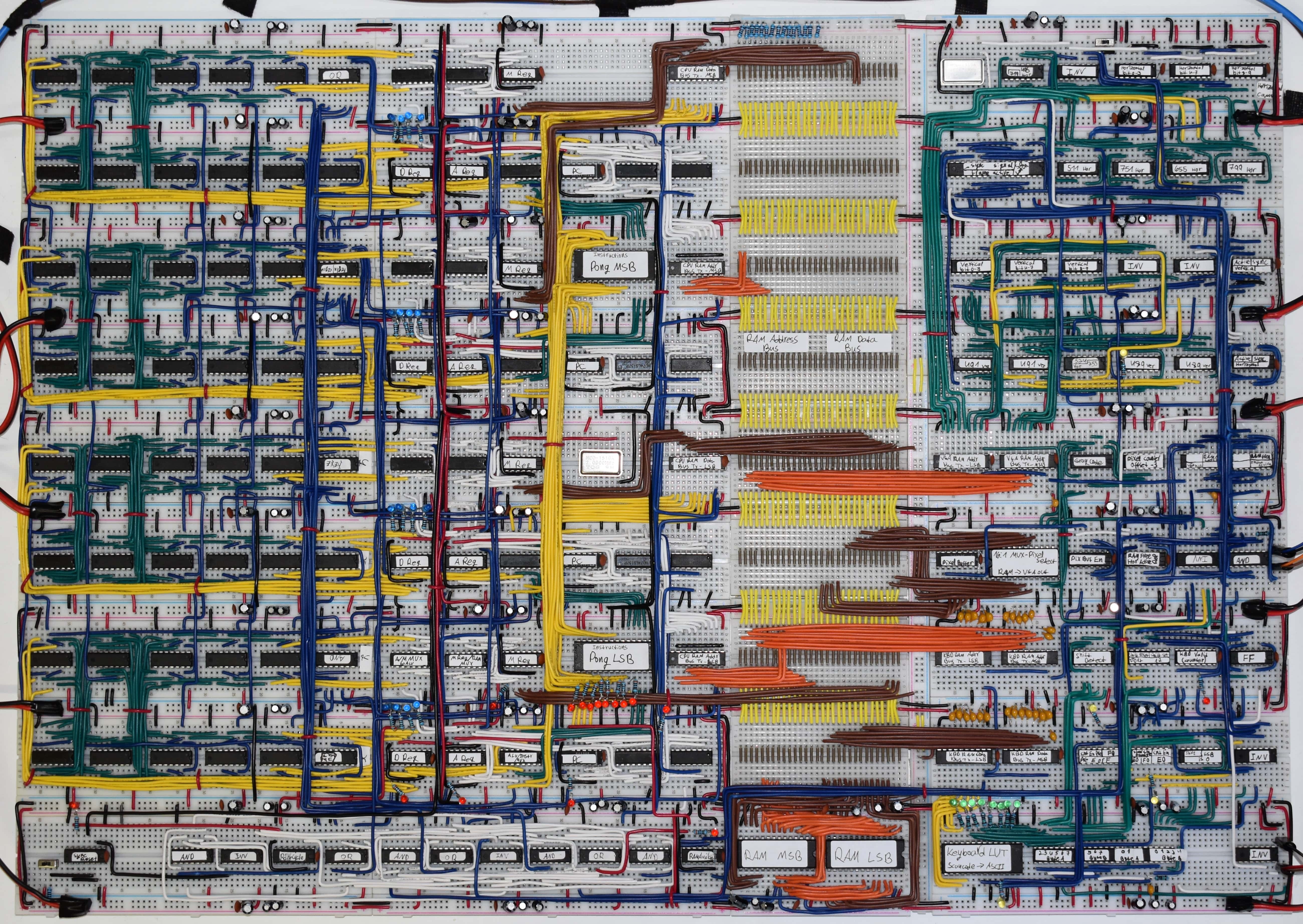
Here is a picture of the final layout of the computer with the functional description of each area.
Now, let's dive into the design and implementation :)
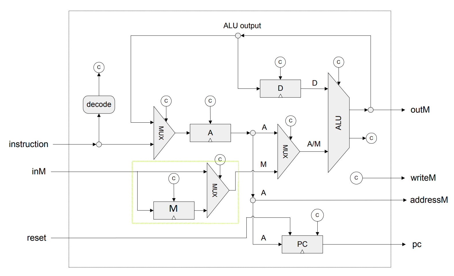
2. CPU
The CPU design is mostly identical to the described CPU in nand2tetris, aside from the addition of the "M Register" and some changes to the control logic. This changes are described in the following sections.
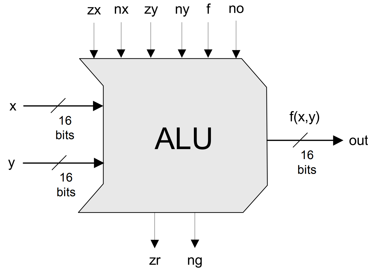
2.1 CPU: Arithmetic Logic Unit (ALU)
The ALU design is identical to what is described in nand2tetris, and is implements as follows:
- x3 = x2 + nx & zx ; x2 = ~zx & x1 ; x1 = x ^ nx
- y3 = y2 + ny & zy ; y2 = ~zy & y1 ; y1 = y ^ ny
- o1 = x3 + y3 ; o2 = x3 & y3 ; o3 = f ? o1 : o2
- out = o3 ^ no ; ng = out[15] ; zr = ~(| out)
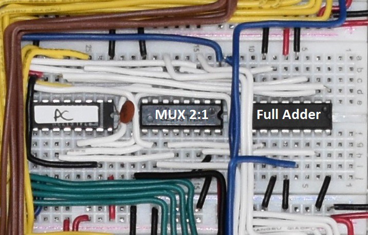
This is the implementation that I found to require the least logic ICs on the breadboards.
The breadboard layout of the ALU is designed as 4 identical slices of 4-bits ICs: XOR, AND, OR, MUX 2:1 and 4-bit Full Adder. This was pretty repetitive to build, but very satisfying when finished :)
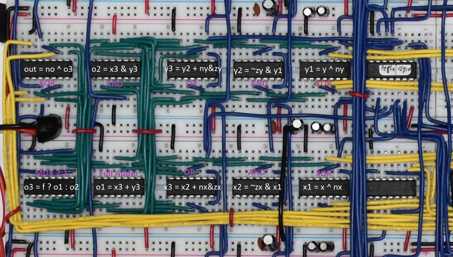
The 2 rightmost ICs in each of the 4 slices are for nx&zx, ny&zy and for calculating zr.
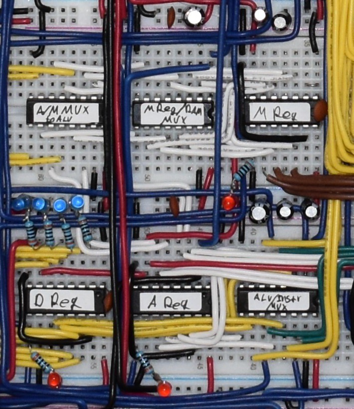
2.2 CPU: Registers (D/A/M)
The CPU registers and MUXs are as described in nand2tetris, except for the addition on the M register as shown in the diagram below. The M register is used to hold data that is read from RAM when executing an instruction that require both read and write from RAM (For example, M=M+1).
This was required as I chose to use RAM chips with a shared data bus for read/write so it is not possible to read and write at the same time. The control logic detects if current instruction requires both read and write, and will execute the instruction in two cycles in that case. At the first cycle, data will be read from RAM and stored in the M register. In the second cycle, data from the M register will be used by the ALU and the output will be written to RAM.
This basically changes the CPU design from single-cycle as proposed in nand2tetris, to multi-cycle CPU :)
The breadboard layout of the CPU Registers and MUXs is designed as 4 identical slices of 4-bit registers and MUXs.
2.3 CPU: Program Counter (PC)
The PC is as described in nand2tetris and is implemented as the following:
- PC <= load ? A : PC + 1
The breadboard layout of the PC is designed as 4 identical slices of 4-bit ICs: registers, MUXs and Full Adders:
2.4 CPU: Instruction Memory
The instruction memory is as described in nand2tetris. I used 2 EEPROM ICs of 8-bit words and 32K addresses (15-bit). The first IC holds the 8 least significant bits of the 32K instructions, and the second holds the 8 most significant bits. One of the ROM chips is located on the top of the breadboards, nearby the two most significant slices (8 upper bits) and the second one on the bottom.
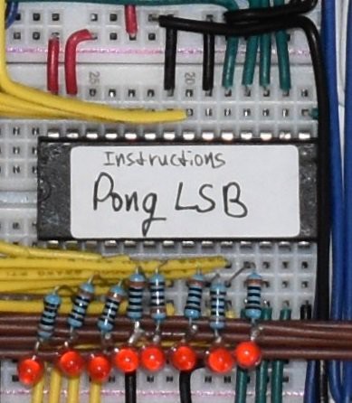
I built an EEPROM writer breadboard that uses an Arduino to flash the instructions into the ROM. I used it to flash the Pong game that is supplied with nand2tetris course as a demonstration of the Hack computer.
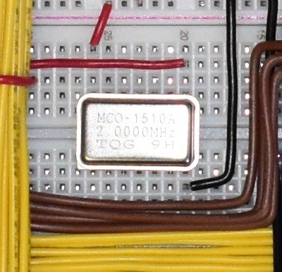
2.5 CPU: Clock
The CPU clock is generated by an active oscillator with frequency of 2MHz. This clock frequency was selected as the critical path of the design is around 500ns. I experimented with a 3.28Mhz oscillator that I have, but Pong ran too fast and the design was not very stable :)
2.6 CPU: Reset
For reset I used a simple switch that acts as an asynchronous reset that is sampled with a flop to output a synchronized reset. The synchronization is to de-bounce the switch, and to make sure the first cycle of the CPU will be of a full duration.
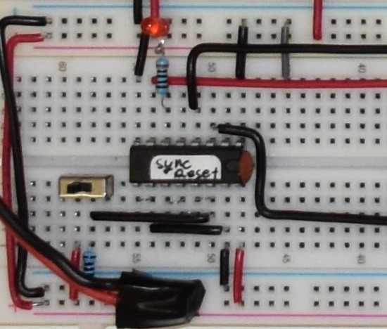
Now that I'm writing this, I realize I should have used a double FF sync instead of single FF, to avoid metastability when exiting reset close to clock positive edge...
2.7 CPU: Control Logic
In this section I describe how the control logic signals in the CPU are constructed. For reference, here are the Hack instruction data read and write bits for C-Instruction (instr[15] asserted):
- instr[3] - Write destination is Reg M
- instr[4] - Write destination is Reg D
- instr[5] - Write destination is Reg A
- instr[12] - Read Source is RAM
Control Logic: RAM Read/Write cycle
As I explained above, the CPU design was adjusted so that instructions that require RAM read and write will be executed in 2 cycles. A way of knowing if the CPU is currently on the read or the write cycles is required. I used a register called "RdWrCycle" that indicates that. It is defined as such:
- Flop in: ~RdWrCycle
- Flop En: instr[15] & instr[12] & instr[3] & RAMAvailable
"RdWrCycle" will be 0 for instructions that does not require both read and write to RAM.
Control Logic: Wait For RAM
Whenever the CPU is not granted RAM access but do require it for the current instruction, a signal named WaitForRAM is asserted. When this signal is asserted, the CPU does not load values into the D/A/M registers, does not increment the PC and does not write to RAM. It is defined as such:
- WaitForRAM = instr[15] & (instr[12] | instr[3]) & ~RAMAvailable
Control Logic: Stall
The CPU needs to not execute (to stall) whenever it needs to wait for RAM, or it is currently in the first cycle of executing an instruction that requires RAM read and write cycles. The stall signal is used by other control logic to allow that.
- Stall = WaitForRAM | (~RdWrCycle & ( instr[12] & instr[3] ) )
Control Logic: CPU Registers
Here are the load conditions for the CPU registers:
- Load D = instr[15] & instr[4] & ~stall
- Load A = ~instr[15] | (instr[5] & ~stall )
- Load M = instr[15] & instr[12] & instr[3] & ~RdWrCycle & ~WaitForRAM
- Load PC = ~stall
Control Logic: Data Path
Here are some signals that control the CPU data path:
- MUX A/M->ALU select signal = instr[12]
- MUX M/inM->A/M MUX select signal = instr[15] & instr[12] & instr[3]
- CPU RAM write = instr[15] & instr[3] & RAMAvailable & (~instr[12] | RdWrCycle)
3. RAM
The CPU, VGA and keyboard all need to share access to the RAM. The VGA must get access to the RAM whenever the VGA controller is actively sending pixel data to the display. For the 512x256 resolution of the Hack computer, and the 640x480@60Hz VGA specification, RAM will be reserved for the display about 30% of the time (More info in VGA section 4.4). That means that only whenever the VGA controller does not require RAM access, the CPU and Keyboard can access it. The VGA controller generates for the CPU the signal "RAM Available" which is sampled by the CPU Control Logic and used to indicate when the CPU should execute and when to stall.
All of the 3 mentioned agents need to be able to drive the RAM's address bus. The CPU and Keyboard needs to be able to drive the RAM's data bus. To allow for multiple agents to drive the same bus, I used bus transceiver ICs that are enabled according to which agents currently granted RAM access, with the following enable signals:
- VGA Addr Bus En = vga_active
- KBD Addr Bus En = kbd_active
- CPU Addr Bus En = ram_avail
- KBD Data Bus En = kbd_active
- CPU Data Bus En = cpu_wr
Refer to each section for the definition of these signals.
The RAM output enable and write enable signals are constructed as such:
- RAM Write En = ~clk & (cpu_wr | kbd_active)
- RAM Read En = ~RAM_Write_En
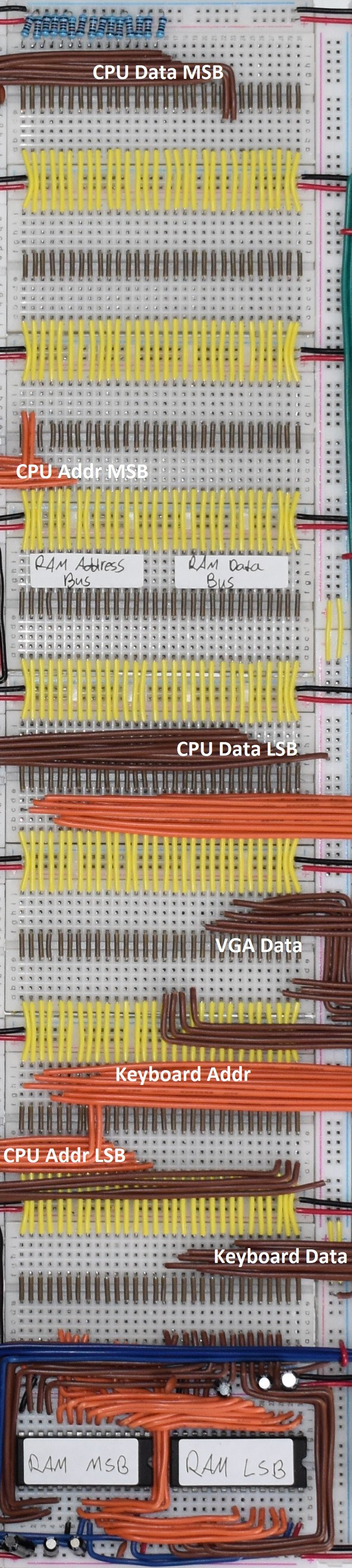
I used 2 SRAM ICs of 8-bit words and 32K addresses (15-bit). There are 3 agents needs to be physically connected to the RAM chips through the bus transceivers, so I noticed it is not going to be possible to wire all of them directly to the RAM ICs' breadboard. To deal with that, I chose to create an address and data buses vertically, using multiple 30-row breadboards between the CPU, and the VGA and keyboard (Inspired from Ben Eater's amazing 8-bit CPU video series). I needed a total of 15-bit (address) + 16-bit (data) = 31-bits bus, so in addition I used a few breadboard power rails to add another 1-bit bus that is vertically accessible to all agents. This way, each agent that needed to be connected to the RAM's address or data pins, can be wired to the bus to avoid wiring mess.
4. Video - VGA
I chose to implement the video output of the Hack computer using VGA. I chose VGA as it requires relatively simple logic, and I've seen people achieve this on breadboards. The VGA controllers I designed follows the VGA 640x480 @ 60Hz timing standard. This resolution and refresh rate standard were chosen as it requires the "slowest" pixel clock (25.175MHz) while supporting a resolution of at least 512x256, as required by the Hack computer's design. Also, this standard seems to be very widely supported. I expected this is going to be challenging, as 25MHz is considered to be on the high end of what is possible on breadboards.
For the VGA controller to work with the display, horizontal and vertical sync pulses of a specific widths and frequencies need to be generated and output to the display, according to the chosen VGA standard. In addition, serial pixel data needs to be output to the display, timed relative to the sync pulses according to the chosen VGA standard.
The Hack architecture expects that the pixel data that the CPU writes to the RAM (In the screen address map) will appear on the display. The mechanism that reads this data from RAM and output it to the VGA display needed to be designed.
The VGA controller I designed consists of the following parts:
- Pixel and line counters (horizontal counter and vertical counter)
- Sync pulse generation (horizontal and vertical)
- "VGA Active" signal generation - Indicates that the VGA currently reads pixel data from RAM
- Used to qualify the pixel data read from RAM so only the 512x256 resolution will be shown
- "RAM Available" signal generation
- Indicates to the CPU that RAM is currently available to access, as VGA doesn't use it
- Accounts for the keyboard's RAM access timeframe
- The signal is timed earlier to compensate for the delay of syncing it to the CPU's clock domain
- Pixel read logic - Read Pixel data from RAM and output it to the display
- Done by reading parallel 16-bit words from RAM and output to the display serially
4.1 VGA: Pixel and Line Counters (Horizontal and Vertical Counters)
The pixel and line counters represent which pixel in what line is currently being output to VGA monitor. The VGA 640x480 @ 60Hz timing standard specifies a pixel clock with frequency of 25.175 MHz, line time of 800 pixel cycles and frame time of 525 lines. That requires a pixel counter (horizontal counter) that counts to 800 and line counter (vertical counter) that counts to 525. The horizontal counter will increment each pixel clock (25MHz) and the vertical counter will increment each line.
In order to count to 800 horizontal (10-bit) and 525 vertical (10-bit), I used two groups of three 4-bit counters chained together. The horizontal counter counts from 0 to 799 and the vertical counter counts from 0 to 524. An indication of 799-horizontal and 524-vertical were made using AND and NOT gates to load 0 into the counters and reset the count.
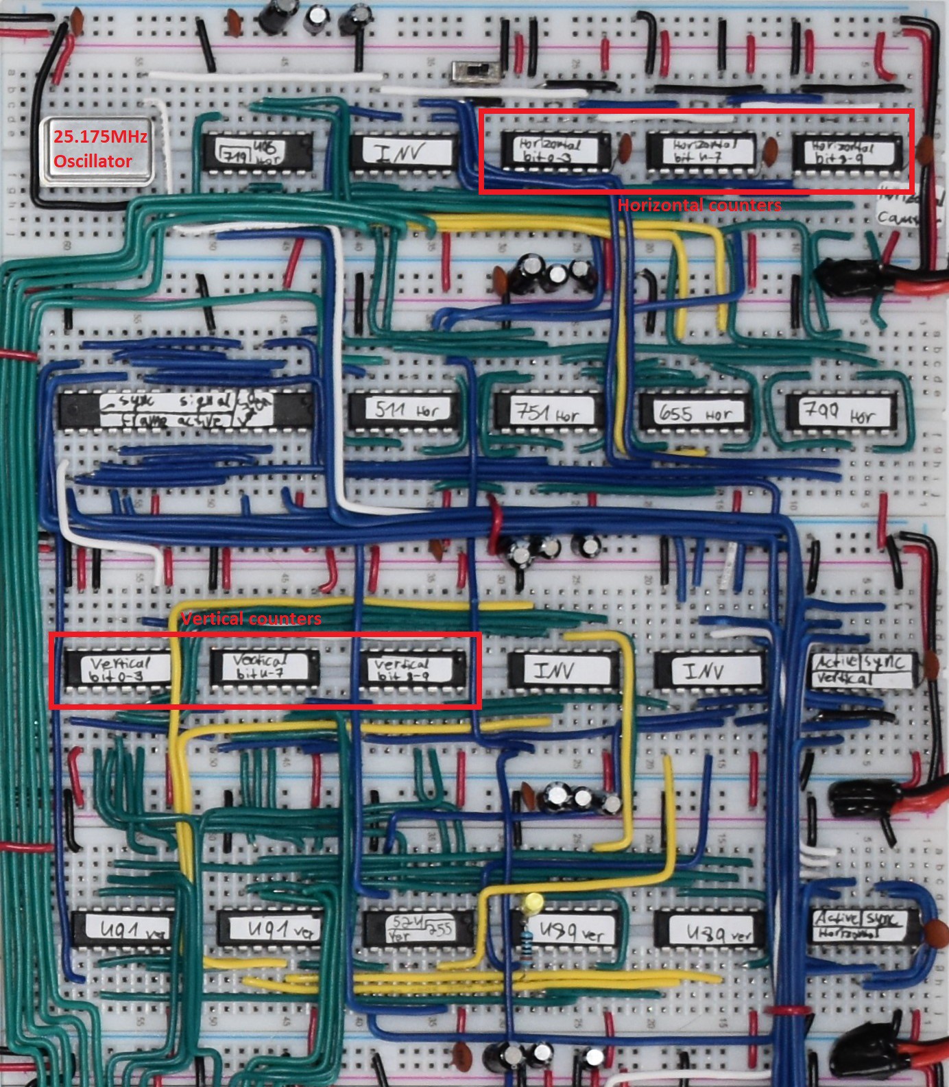
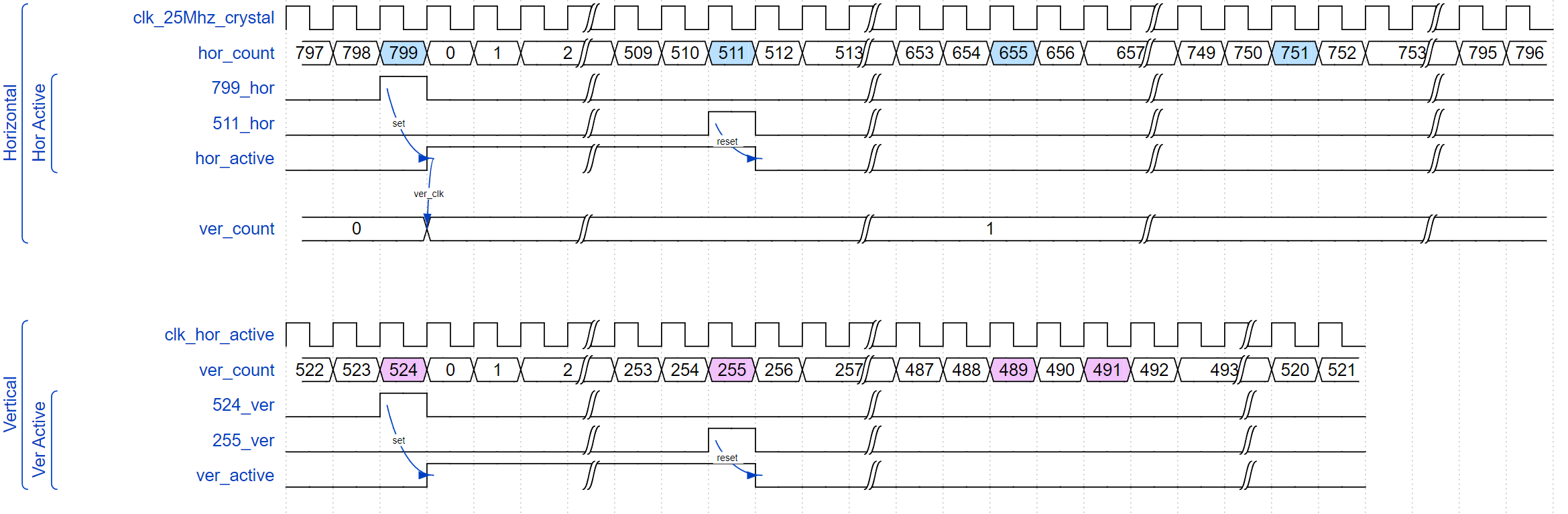
4.2 VGA: Sync pulses
The VGA 640x480 @ 60Hz timing standard require a negative sync pulse between horizontal counts 655 to 751. A set-reset latch is used to create this signal with indications for 655 and 751 horizontal using AND and OR gates.
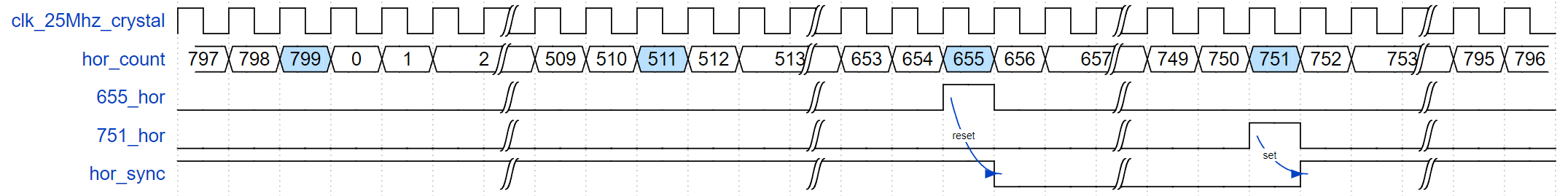
The standard also requires a negative sync pulse between vertical counts 489 to 491 that is built the same way as horizontal sync pulse.
These sync pulses are an output from the design to the VGA connector. With these generated, the display will detect the proper resolution and refresh rate that the design operates at.
4.3 VGA: VGA Active signal
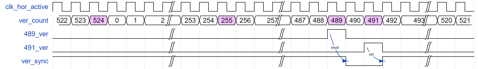
The nand2tetris design specifies an unusual resolution of 512x256 and the VGA timing standard I chose specifies a bigger resolution of 640x480. That means we only need to output pixel data to the VGA display when the pixel counters are within the 512x256 resolution. At all other times, we need to not output any pixel data to the VGA display. To accomplish that, I chose to generate a signal called "VGA Active" that will be asserted only when we the counters are within the 512x256 resolution.
I created two signal called "Horizontal Active", which is asserted between horizontal counts 0 and 5111, and a signal called "Vertical Active", which is asserted between vertical count 0 and 255. The AND of these signal is "VGA Active" and it will be AND with the actual serial data that is output to the VGA display.
Also, the signal "Horizontal Active" is used as the clock for the vertical counters, as it is asserted whenever a newline is started :)
4.4 VGA: RAM Available signal
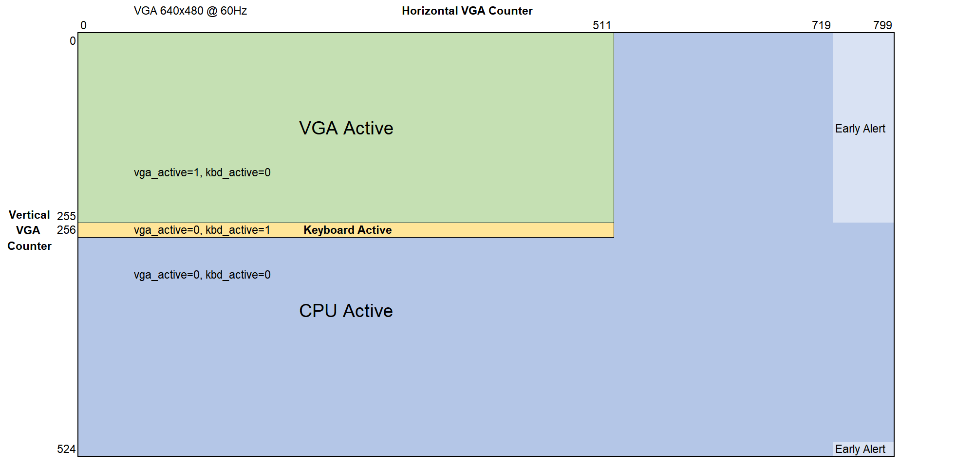
"RAM Available" is a signal generated by the VGA controller and used by the CPU as an indication that RAM is available for access by the CPU (RAM is not used by VGA or keyboard). The RAM is used by the VGA during horizontal count 0-512 AND vertical count 0-255. The RAM is used by the keyboard during horizontal count 0-512 AND vertical count 256.
This signal is similar to the NOT of "VGA Active", but as it is generated in the VGA controller's clock domain (25MHz) and used by the CPU's clock domain (2MHz), it needs to be generated early and synchronized with double flip-flop. Synchronizing "RAM Available" with double flip-flop adds between 1-3 CPU cycles of latency to the sampled signal. That will be problematic if the VGA controller will dis-assert "RAM Available" just when the VGA needs access to RAM, as the CPU will still be using the RAM for an additional 1-3 CPU cycles until the indication is received (10-40 VGA cycles).
To solve that, I chose to assert "RAM Available" each line at horizontal count 719, and dis-assert it at horizontal count 511. In addition to these horizontal set and reset conditions I also wanted to make use of the vertical lines that are not used by the VGA controller. The VGA controllers require RAM access at lines 0-255 and the keyboard uses RAM during line 256. "RAM Available" will not be asserted at all during lines 257-254 so the CPU could maximize its RAM grant time.
Here is the complete set and reset conditions to the "RAM Available" signal:
- "RAM Available" set: 511-horizontal
- "RAM Available" reset: 719-horizontal & ("Vertical Active" | 524-vertical)
The following chart visualizes which agent is granted RAM access according to the VGA's timing. "RAM Available" can be seen as "Early Alert" in this diagram.
4.5 VGA: Pixel data
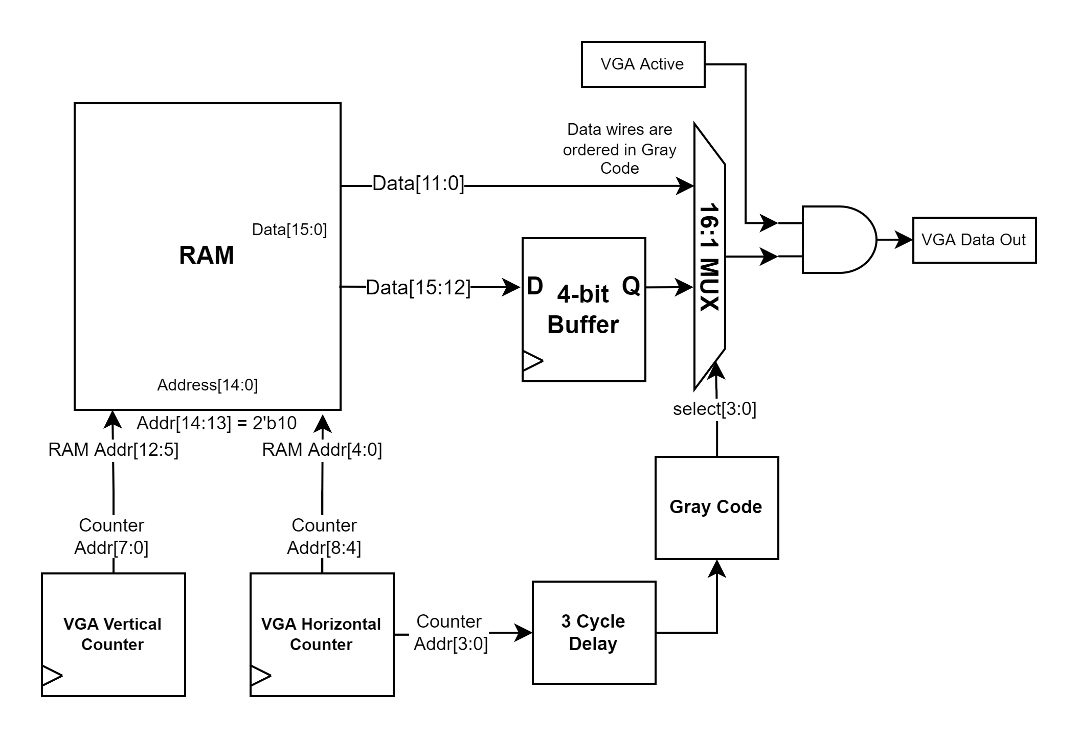
The Hack computer architecture dictates that the screen's pixel data will be stored within RAM address range 0x4000 to 0x5FFF. In each RAM location there are 16 bits of data, representing 16 black and white pixels on the display. The pixel data in the Hack's RAM are ordered the same way as the VGA expects the data to be sent to it, where the least significant bit in the first RAM address represents the top left pixel on screen.
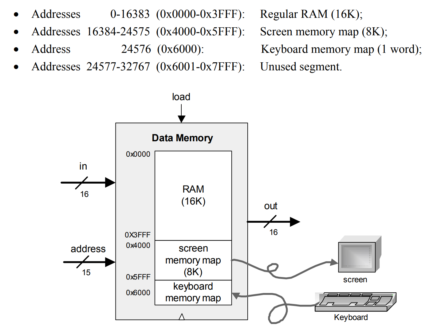
Connecting the VGA horizontal and vertical counters to the RAM's address pins will allow to read the ordered pixel data from RAM and send it to the display. Here is the mapping between the VGA counters and RAM address pins:
- ram_addr[14] = constant 1
- ram_addr[13] = constant 0
- ram_addr[12:5] = vertical_count[7:0]
- ram_addr[4:0] = horizontal_count[8:4]
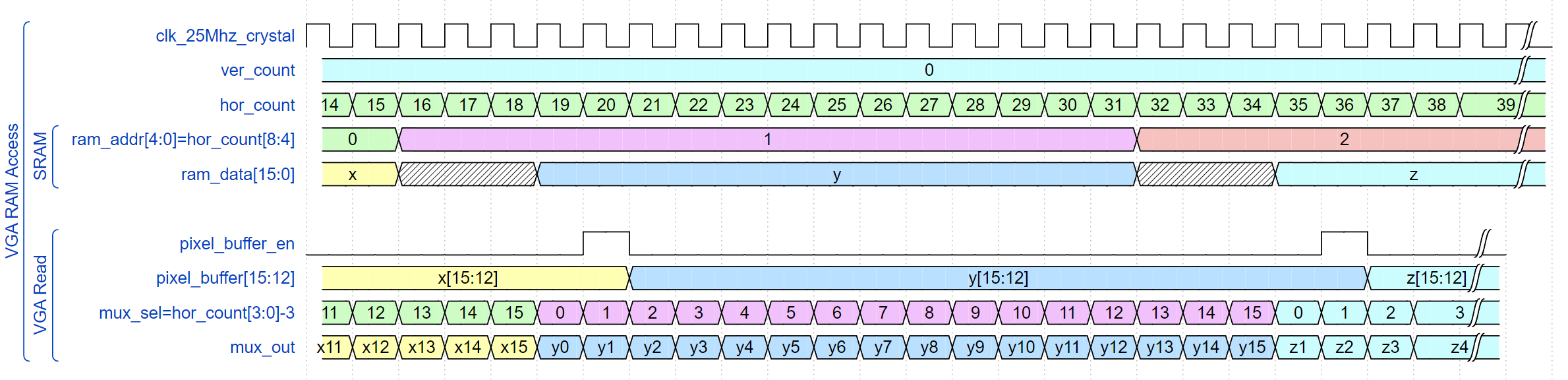
For each of the addresses, the actual 16-bit of pixel data are presented in parallels on the RAM's data pins and needs to be serially sent to the display through the VGA connector. To do that, I chose to use a 16:1 MUX IC, whose 4-bit select pins are connected to horizontal_count[3:0]. That way, the horizontal and vertical VGA counters are used to select all addresses and all pixels in order, and the pixels are serially sent to the VGA.
It may seem that this design is enough to read pixel data from RAM and send it to the VGA, but I encountered 2 problems with this design that are related to timing:
Problem 1
I noticed glitches on the 16:1 MUX output when going through a specific address' pixel data that appeared on the display as visual artifacts. These were the result of the MUX's select signal that is counting from 0-15. With each transition from one number to the next, the 4 bits are changing in slightly different timings, which results in a temporarily wrong MUX selection.
The first solution that came to mind when dealing with glitches from counting was using Gray Code, which is a method of ordering binary numbers such that only 1 bit is changed from one number to the next. I used Gray Code to solve the described problem by converting the MUX's select signal to Gray Code in one end, and connected the MUX's inputs to the RAM data pins in a complementary manner.
Problem 2
It takes the SRAM IC that I chose to use about 100ns from selecting an address until the data appears on the pins, which is about the duration of 2.5 pixel clock cycles. That means that if the proposed design above is to be used, the first 3 pixel in each address will be wrongly presented on the monitor.
To solve that I decided to add a delay of 3 cycles between the VGA counters that are connected to the RAM's address pins, and the actual read from RAM's data pins. To allow that, I added a 4-bit register that acts as 4-bit pixel buffer. This buffer will hold that last 4-bits of each 16-bit RAM data so that the RAM address can be safely changed and the data is unstable.
The first 12-bits of the RAM data are connected directly to the 16:1 MUX, and the last 4-bits of the RAM data are connected to the input of the buffer, whose output is connected to the MUX. To support that, the MUX's select signal was delayed by 3 cycles, as well as the "VGA Active" signal, which is qualified with the actual pixel data before it is output to the VGA connector.
Here are wave diagram and a schematic of the VGA data read design:
Finally, the serial pixel data is AND with "VGA Active" and then goes through a 150 Ohm resistor to the RGB pins of the VGA connector, to display a white-on-black image on the display.
5. Keyboard - PS2
5.1 KBD: On the PS2 protocol
I chose to implement the keyboard input of the Hack computer with PS2. Like VGA, PS2 requires relatively simple logic and I've seen people implement it on breadboards before. The PS2 keyboard interface consists of a data and a clock pins. The clock is generated by the keyboard itself and is held high when the keyboard is idle. When an event occurs on the keyboard (button press are release) packets of 11-bits are sent on the data pin with an accompanying 11 clock pulses. These 11-bit packets consist of 8-bits of data and 3-bits of control (start, stop and error correction bits).
The 8-bit data in each packet, which is called a Scan Code, is used to describe the event happening on the keyboard. One Scan Code may describe an entire event or a part of an event. The are 2 types of Scan Codes: Make Codes and Break Code. Make Codes describe a key press and Break Codes describe a key release. Make Codes are mostly described by 1 packet (8-bits of data) and Break Codes are mostly described by 2 consecutive packets of data. As I understand, the commonly used Scan Code set is set 2, and this will be the one I will be referencing here.
For a specific key described by a specific 8-bit code, the Make Code will include that exact code. The Break Code for that specific key will be "0xF0", followed by the same code from the Make Code. For example, pressing the "A" key on the keyboard will generate 1 packet with the code "0x1C" and releasing the "A" key will generate 2 consecutive packets, whose codes represent "0xF0, 0x1C". For some special keys, the additional code "0xE0" is sent before each key press or release, extending the Make Code to 2 codes and Break Code to 3 codes. These special keys are the arrow keys and Home, End, Del, etc. For example, Pressing the Home key will generate 2 consecutive packets, whose codes represent "0xE0, 0x6C" and the Break Code will be "0xE0, 0xF0, 0x6C".
The Hack computer architecture method of interacting with the keyboard is by reading the RAM address 0x6000 which is assumed to store the ASCII value of the currently pressed character, or 0x0 when no key is pressed Note that the ASCII value and the Scan Codes are different and does not map 1 to 1. Moreover, there are characters that are produced by using the Shift key on the keyboard together with another key. A conversion mechanism is needed from PS2 Scan Codes to ASCII characters.
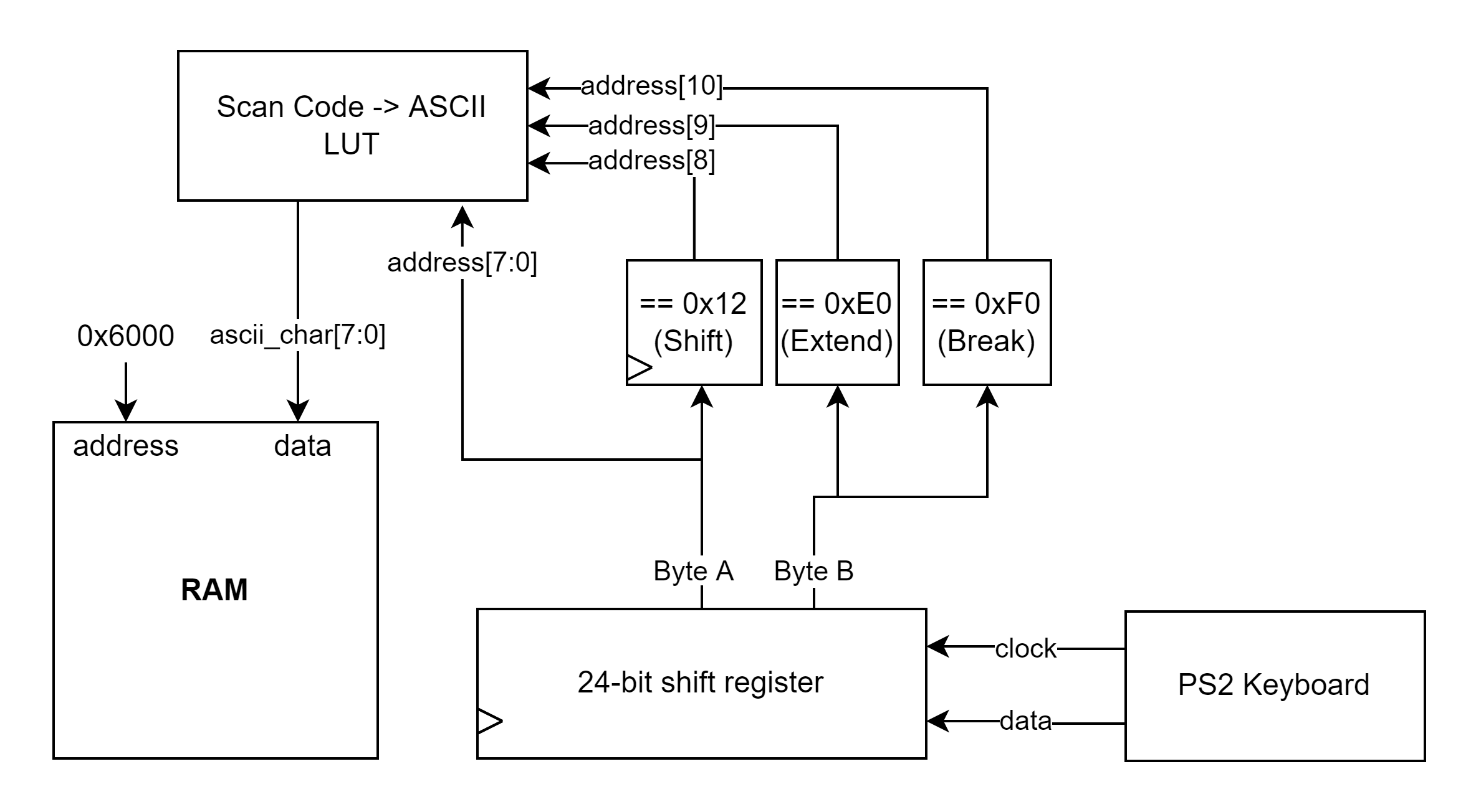
5.2 KBD: Decoding Scan Codes
I chose to implement the keyboard interface such that on a key press, the corresponding character is written to RAM, and on any key release, 0x0 is written to RAM. This way, I don't need to check which key is released when I detect a Break Code. This enables the design to require only the last 2 codes (A and B) to decide on an action, according to this table:
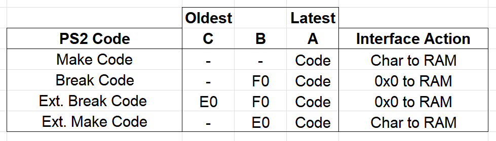
When 0xF0 is detected on Byte B, the event is decoded as a break code and thus it is not needed to decode Byte C.
To implement that I used 3 cascaded 8-bit shift registers that holds the last two 11-bits (22-bit total) packets arrived from the keyboard PS2 connector. A "Ext" and a "Break" signals are made by comparing Byte B to 0xE0 and to 0xF0 respectively. In addition a register was used to store whether the Shift key is currently pressed. These 3 signals (E0, F0, Shift) together with the Make Code stored in Byte A are then used as the address of a ROM programmed to translate the PS2 codes to ASCII character, acting as a Look-Up table (LUT). The LUT is connected as follows:
- lut_address = {break, ext, shift, code[7:0] }
Whenever break is asserted, the LUT outputs 0x0. When break is not asserted, each address stores the relevant ASCII character associated with ext, shift and code[7:0]. The ROM is flashed with a conversion table I made and is attached to this project.
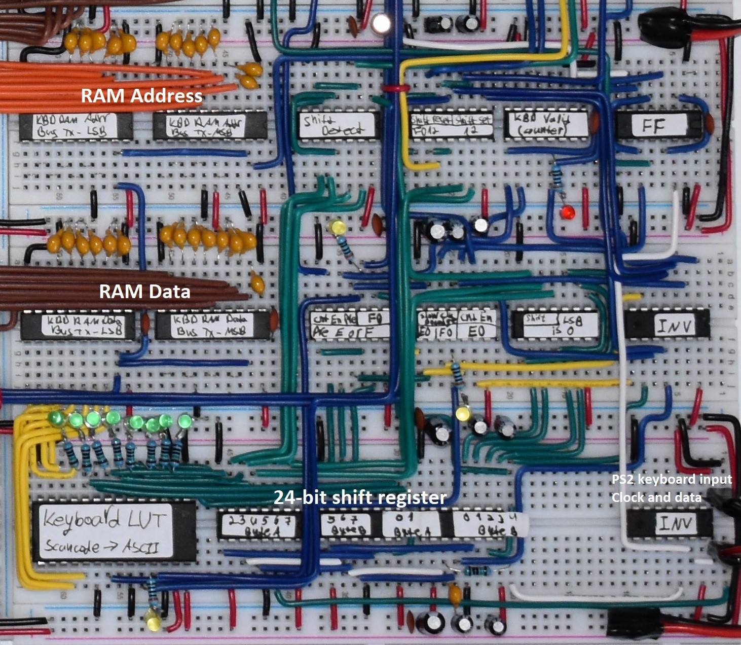
Here are the block diagram and breadboard layout of the keyboard controller design:
5.3 KBD: Keyboard Valid
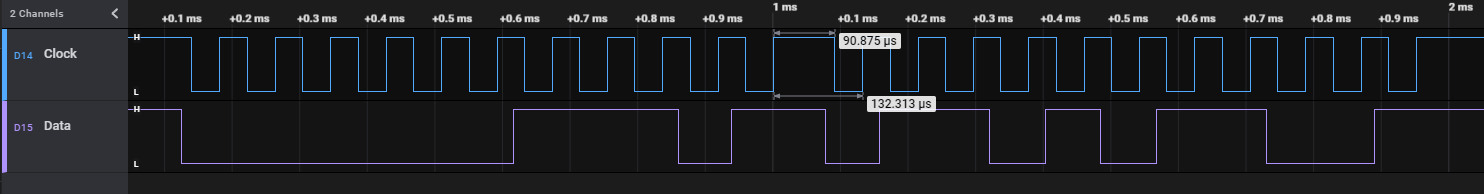
A way of knowing when a Scan Code sequence is done is required, so that the translation to ASCII and the write to RAM will be done on correct data. It is known that when a packet is sent from the keyboard, 11-bits are expected, but it is not known how many packets. I measured less than 100 micro-sec between packets on my keyboard, so that known delay can be used to wait for the sequence to end:
I designed a mechanism that checks if a packet sequence has concluded or not, named "Keyboard Valid". The idea is to check if the keyboard's clock hasn't been low for a duration greater than the time between two packets. I used a counter that asserts "Keyboard Valid" whenever it reaches the number 2. This counter is reset to 0 each time the keyboard's clock is low (data is currently being sent), and increments whenever the keyboard's clock is high AND a slow toggling signal is asserted. The slow toggling signal must be slower than the time between two packets. I used one of the VGA vertical counters (vertical_counter[2]) which toggles with a cycle time of about 130 micro-sec, which is greater than the 100 micro-sec delay between packets that I measured. The counter itself is clocked by the VGA's 25MHz clock. Here is a wave diagram that visualizes the behavior:
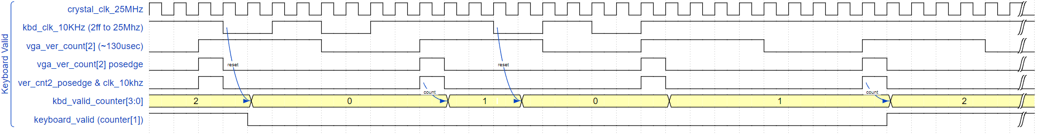
This "Keyboard Valid" signal is used to clock the storage register of the shift register, making that output data only change when a keyboard event as concluded. This make sure we don't write to the RAM garbage.
5.4 KBD: Keyboard Active
The keyboard ASCII value will be written to RAM when the VGA vertical counter is on line 256 (right after VGA itself finishes drawing the frame) AND there is a valid character to be written:
- kbd_active = 256-vertical & horizontal_active & kbd_valid
Refer to section "VGA: RAM Available" for more info about timing where the keyboard is granted RAM access.
6. Power Delivery
I had many, many problems with power delivery. It took me some time to realize that a simple 5V/2A cell-phone charger connected to the corner of the breadboards was not going to be enough.
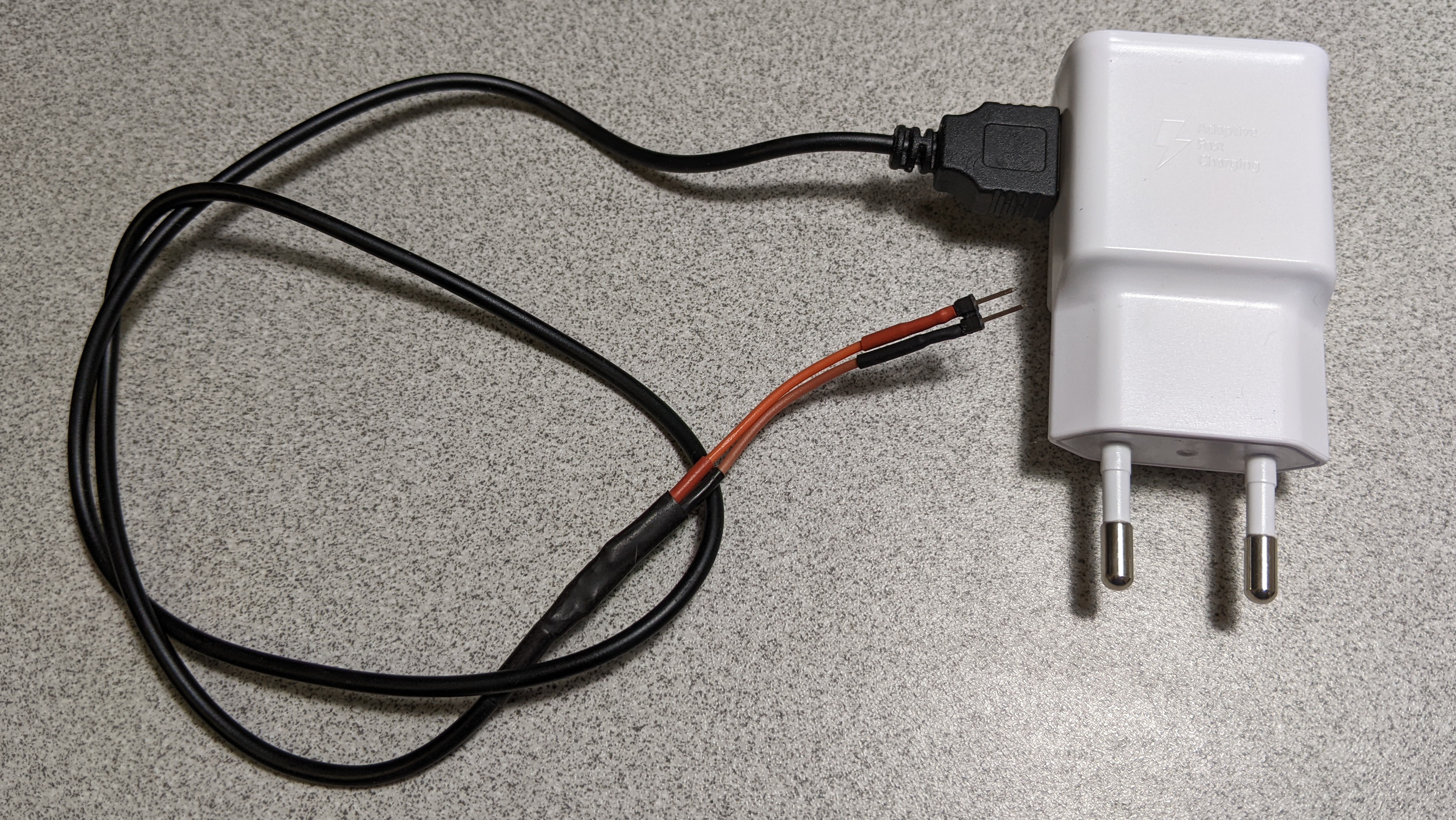
I understood that I have two issues. The first issue was voltage drop across the thin cable and across the many breadboards. I understood that I need both a thicker cable between the power supply and the breadboards, and also I need multiple attach points to the breadboard. The second issue that I had was current draw. I summed the peak current draw of all the ICs on the breadboards and the result was around 10A (on 5V). I guess that this peak draw may not occur on all the ICs simultaneously, but around clock pose-edge I expect an amount close to it. My poor 5V/2A charger and thin cable were not up for the task.
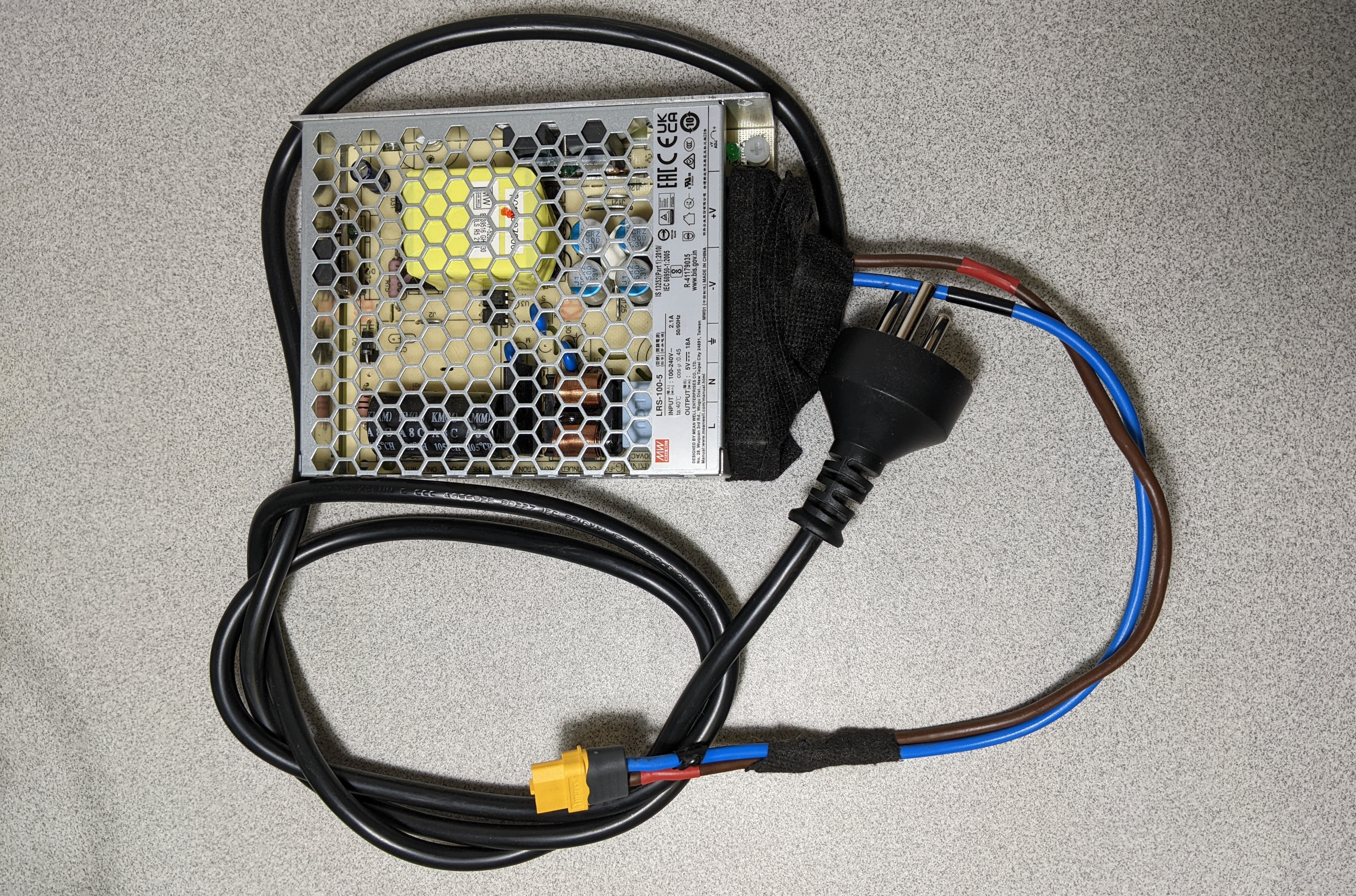
To solve these problems, I designed a power delivery solution that consists of the following elements:
- 5V/20A power supply with fine voltage adjustment knob
- Multiple power cable entry points to the breadboards
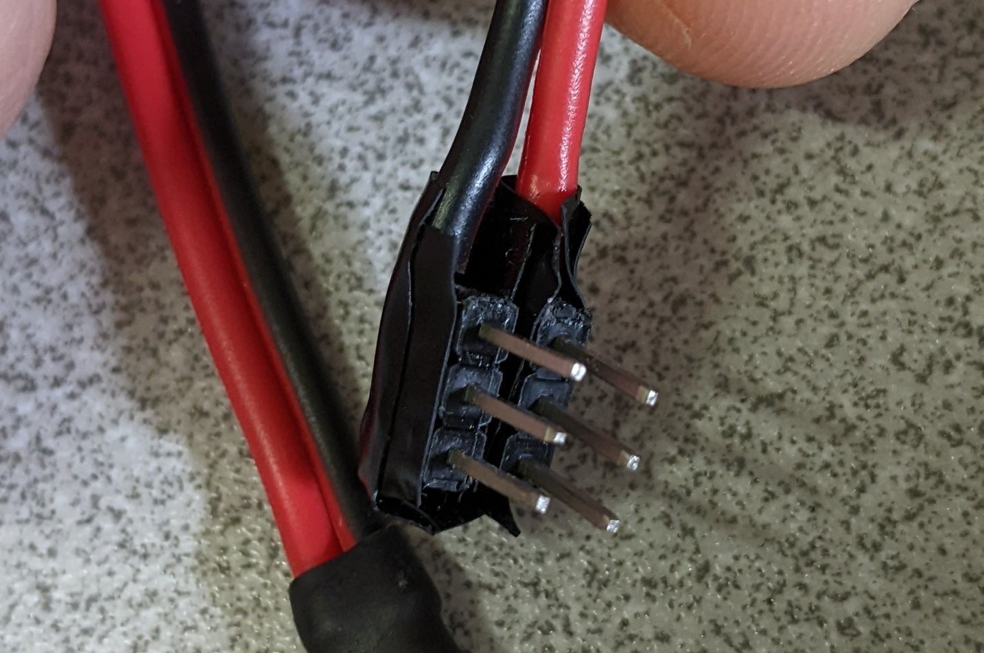
- Each entry point is using 3 pairs of pins to connect between the cable and breadboard
- 12 Gauge power cables between the power supply and split point
- High current XT60 power connector
- Filter capacitors on each of the breadboards (1uF, 10uF, 100uF) to stabilize the voltage level
- Decoupling capacitors on many of the sequential ICs (0.1uF)
7. Components
Here is a table of the IC models I used and how many are used in each logical unit:
| IC name | IC model | ALU | CPU Control | CPU | VGA | Keyboard | Total ICs |
| 32k x 8-bit EEPROM | AT28C256 | 2 | 1 | 3 | |||
| 32k x 8-bit SRAM | CY62256 | 2 | 2 | ||||
| 4-bit Counter | 74LS161 | 7 | 1 | 8 | |||
| 4-bit Full-Adder | 74LS83 | 4 | 4 | 8 | |||
| 4-bit Register | 74LS173 | 3 | 16 | 5 | 1 | 25 | |
| Hex 1-input NOT | 74LS04 | 2 | 4 | 2 | 8 | ||
| Quad 1:2 MUX | 74LS157 | 4 | 16 | 20 | |||
| Quad 2-input AND | 74LS08 | 16 | 4 | 13 | 3 | 36 | |
| Quad 2-input OR | 74LS32 | 12 | 3 | 2 | 2 | 19 | |
| Quad 2-input XOR | 74LS86 | 12 | 1 | 13 | |||
| Octal Bus Tx | 74LS245 | 4 | 2 | 4 | 10 | ||
| Single 1:16 MUX | 74150 | 1 | ; | 1 | |||
| Shift Register | 74HC595 | 3 | 3 | ||||
| Total | 48 | 12 | 44 | 35 | 17 | 139 |
I also used the following components:
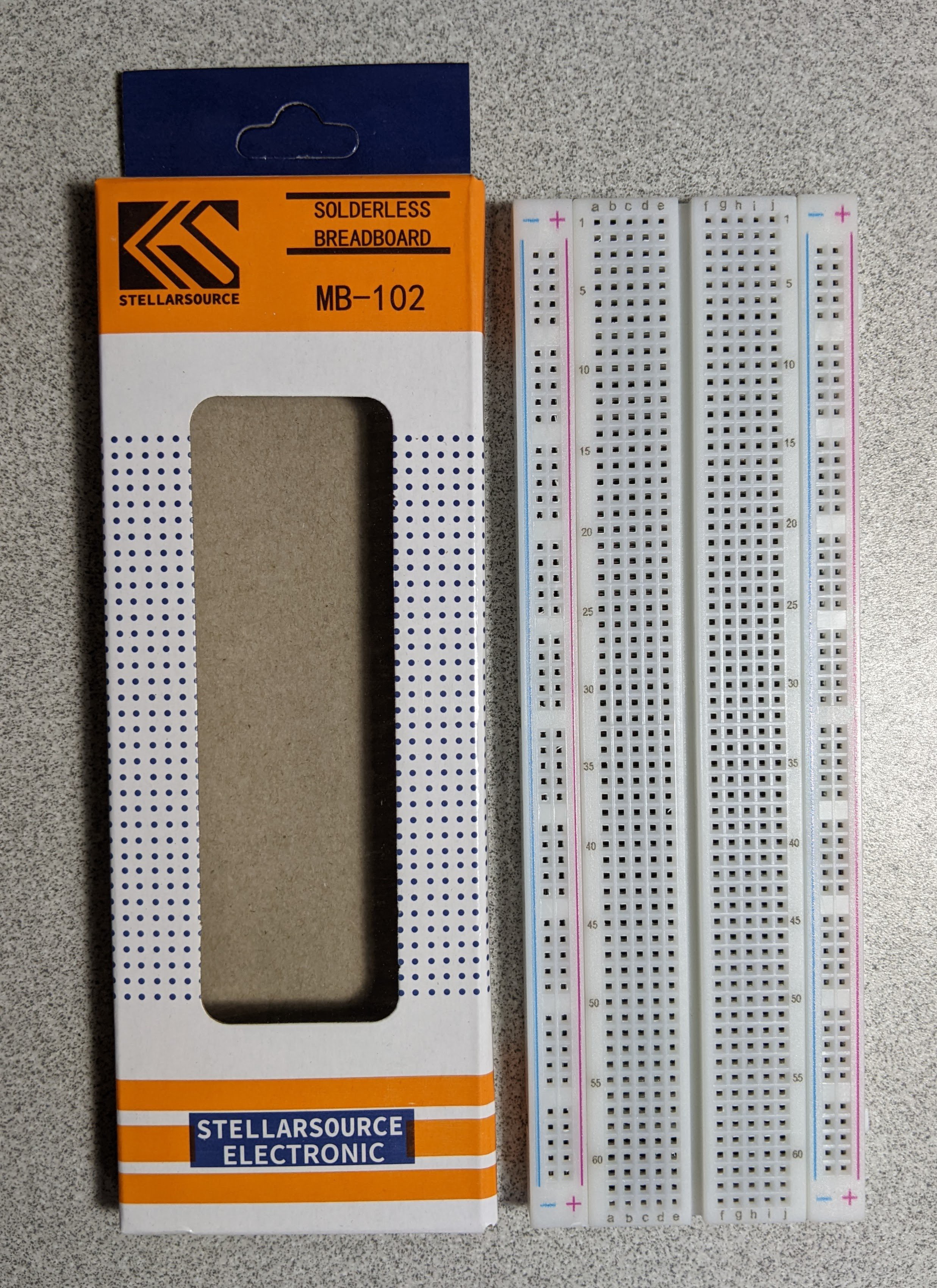
- 27 Long breadboards (Stellarsource Electronics MB-102)
- 9 Short breadboards
- 25.175Mhz Active Oscillator
- 2Mhz Active Oscillator
- 5V/20A Switching power supply (LRS-100)
- 22 AWG solid-core wires for the breadboard (total length of about 150 meters)
- VGA And PS2 connectors
- Resistors and capacitors of various values
- 3mm LEDs
- Switches
And for debug I used the following tools:
- 16 channels 100MHz Logic Analyzer (off-brand)
- 4 channel 50MHz 1GSa/s Oscilloscope (Rigol DS1054Z)
Here's a picture of the breadboards I bought:
That's all :)
Feel free to contact me here or send me an email at tomer.kronik@gmail.com.