 sandy
sandyCD4017-LED-Chaser-circuit

An LED chaser or LED running light can be used as a decorative light, fancy light, chasing taillight for vehicles, etc.
The circuit consists of a 555 astable multivibrator circuit and a 4017 counter using IC. The output of the 555 generates a square wave
or clock input for the decade counter. For each positive edge triggering of the clock input,
the counter shifts the high state of the output in a sequence from output 0 to output 9.
In a 4017 counter IC, only one output will be high at a time and the remaining outputs will be in the low state.
And the shifting cycle repeats like a ring counter. Thus the LEDs will visually seem like a rotating.
COMPONENT USED
IC 555 :- https://amzn.to/2PyeshF
IC 4017 :- https://amzn.to/2o5NWQs
LED :- https://amzn.to/2wj3Meb
10K POT :- https://amzn.to/2MRiTWe
10uF CAP. :- https://amzn.to/2MRkdZc
CUTOM PCB from JLCPCB

CIRCUIT DIAGRAM


Here the Chaser circuit is designed with an ON time of 0.047s for each LED.
The speed of the chaser can be varied by adjusting the time period of the clock input.
That is the time period of the 555 astable multivibrator circuit, which can be calculated as T = .69 (R1+2R2) C.
You can see that the 555 timer wired as an astable multivibrator and its output is connected to the clock input of 4017 counter IC.
The output frequency of the 555 timer is determined by the resistors R1, RV1 and capacitor C1. VCC (8th pin) and GND (1st pin) is connected to the power supply.
Reset (RST – 4th pin) is connected directly to the positive power supply to avoid accidental reset of 555 timer.
Control Voltage (CV – 5th pin) is not used, so to avoid high frequency noises we are connecting a capacitor (C2 – 0.01μF) to the ground.
LED D1 is used to indicate the output of 555 IC and the resistor R3 is for current limiting.
Similarly VDD (16th pin) and VSS (8th pin) of the CD4017 IC is connected directly to the power supply. Clock enable (13th pin) is an active low input,
so it is connected to ground. Clock input (14th pin) is connected to the output of 555 timer. Each decoded output pins (Q0 ~ Q9) is connected to LED.
Resistor R3 is used for current limiting. Only one resistor is required for limiting current through all LEDs since only one LED will turn on at a time.
ORDERING PCB


First of all I design the PCB in Easy EDA PCB designing platform I have order PCB from JLCPCB because JLCPCB have very affordable rates for PCB
like only 2$ for 1 - 4 layer PCB, you will get high quality PCB FROM JLCPCB in very short time you can surly can consider JLCPCB for your future PCB needs.
I am very happy and satisfied with the PCB quality I surly go with JLCPCB for my Next PCB order.
and If you register yourself today on JLCPCB you will get wellcome coupons worth of 30$ exclusively Now no need to order components separately for you PCB and get free from stress of soldering them on PCB just try PCB SMT assembly service and get you PCB with components pre assembled ready for the project
For more detials & offers please visit JLCPCB.com

First I solder the IC base on PCB, there are total 2 IC base in this project
8 pin base for IC 555 & 16 pin base for 4017 IC


Using base for IC is good practice instead of directly soldering IC to the base
because in future if accidently our IC got burn its very much easy to replace them.
Then I slodered some small components like Capacitor, resistor and power LED to the PCB

Then I solder this 10k ohm potentiometer to the PCB
this the magic component of this project by rotating this potentiometer we can change the LED chaser speed.
basically the change in resistance provided by this potentiometer the charging and discharging time of
capacitor is changed due to this IC 555 IC delivery variable Square wave to IC 4017

Then I placed our both IC’s, which are IC555 and IC4017
I powered this LED...
Read more »
 Sagar 001
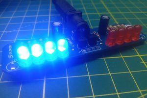
 ElectronicABC
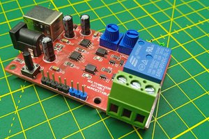
 tomcircuit