This project has a few goals:
1. Use cheap and easily available 74xx chips. The higher numbered 74xx chips are expensive and hard to come by in small quantities. It may require more chips, but the overall price will be lower. The low number 74xx chips are less than a dollar, while the higher numbers chips can be between $4-$16 or more. I'd much rather use an 8-bit counter than a 4-bit counter, but I can't reasonably get my hands on it. And I don't want to buy from eBay.
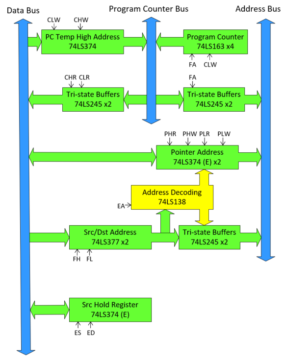
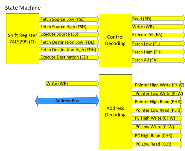
2. I think it's ok to replace some of the chips with wired-or/and gates. The addressing decoding would require a lot of gates which is why so many old computers used a programmable PLA chip to do this. I'd rather stay away from programmable PLAs or FPGAs for this project. Which is why there will be massive arrays of diodes.
3. The Gigatron taught me that programming video timing is very not fun ("racing the beam"). When the processor is in charge of the video timing, any code must be timing precise. When you are debugging code, and it messes up your display, it's very annoying. I just want to worry about the program when I'm programming. So that means independent timing for the VGA output. This increases the chip count, but makes it much more fun to program. Since this is a hobby project, fun is the priority. If it was a computer to sell by the millions, then price would be the priority instead.
Development plan:
I will develop first on a FPGA development board using structural code. So I'll write the code for the 74xx chips, and then connect them in the top level design just like the schematic. I can simulate the operation in the FPGA simulator, and then synthesize and download onto my Basys3 board. The Basys3 has enough internal memory and has a VGA output. It also has some switches and LEDs that I can use for development. Maybe the first peripherals. It also has a UART port for that peripheral. I use a lot of floating busses which the FPGA can't do, so it's not a perfect replica.
When I'm happy with the FPGA operation, I may make a solderless breadboard prototype, and then get a PCB fabricated.
 Foxchild
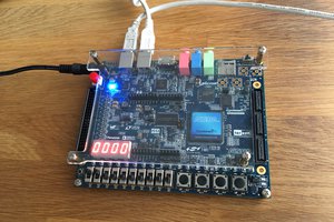
 ErwinM
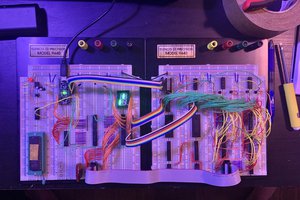
 Tim Ryan
 agp.cooper