0%
0%
Marklin Turnout Controller
Marklin Turnout Controller
 StephanStrassleRojas
Become a Hackaday.io member
Already have an account? Log in.
Just one more thing
To make the experience fit your profile, pick a username and tell us what interests you.
Pick an awesome username
hackaday.io/
Your profile's URL: hackaday.io/username. Max 25 alphanumeric characters.
Pick a few interests
Projects that share your interests
People that share your interests

 agp.cooper
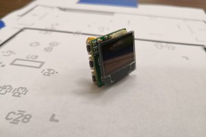
 Mark Omo
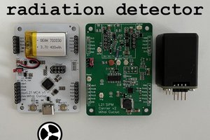
 mihai.cuciuc
 Christoph Tack
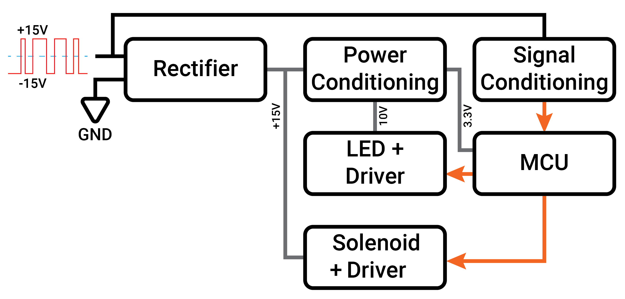
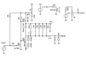
great stuff. I would love to try this at home :) did you publish the schematic and code anywhere? What mcu did you end up using? The board looks really compact.