 utsourceproduct
Today I will show to how to make How to make 500W Step up converter
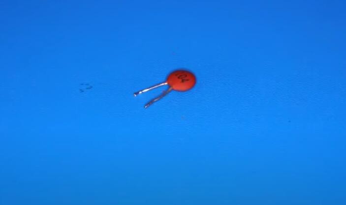
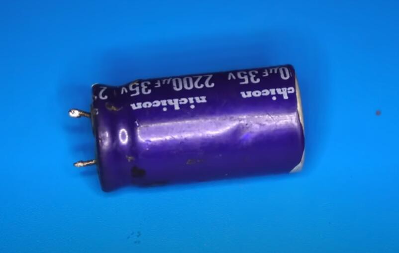
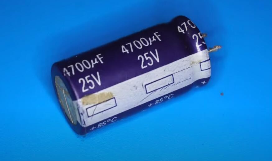
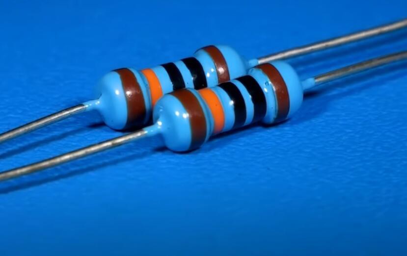
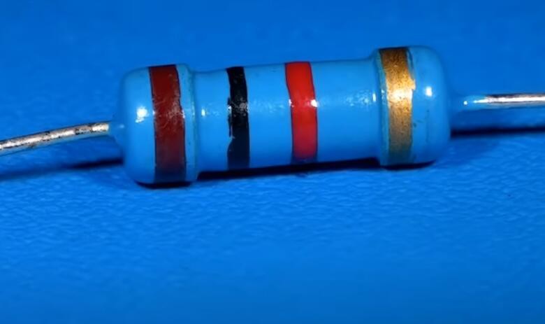
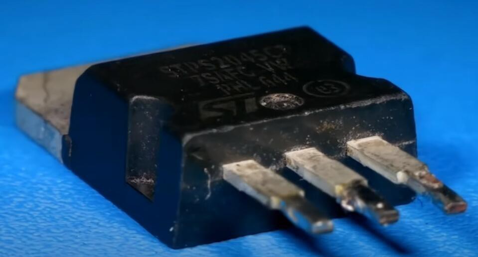
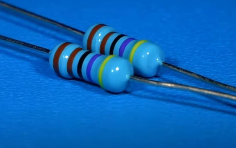
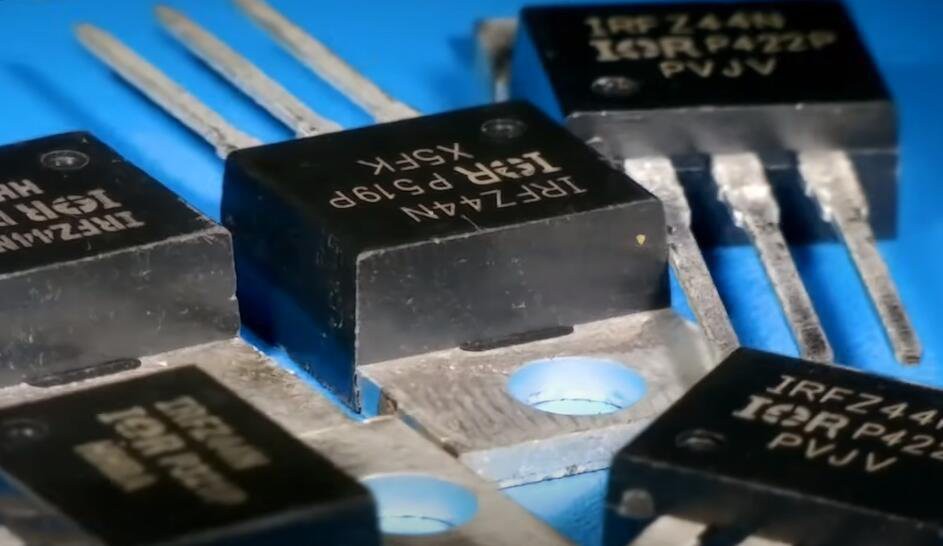
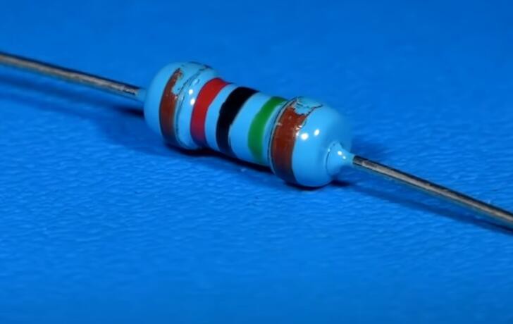
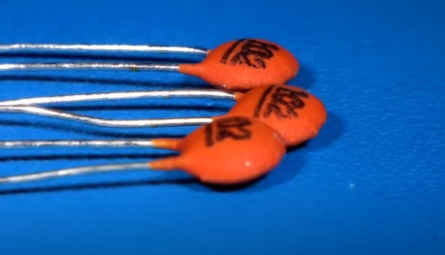
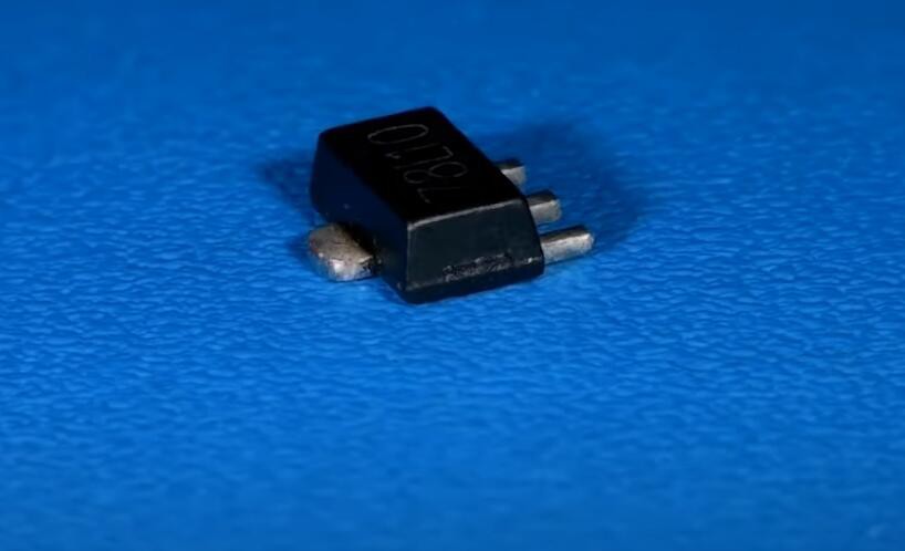
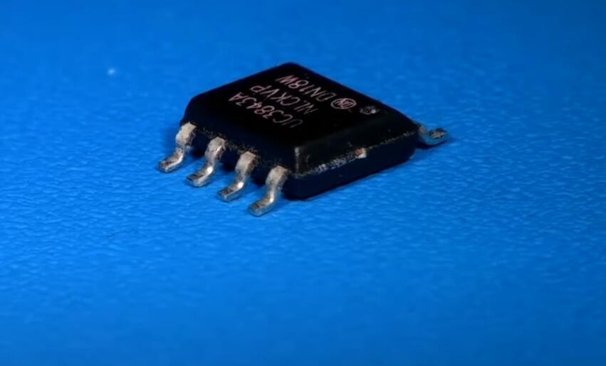
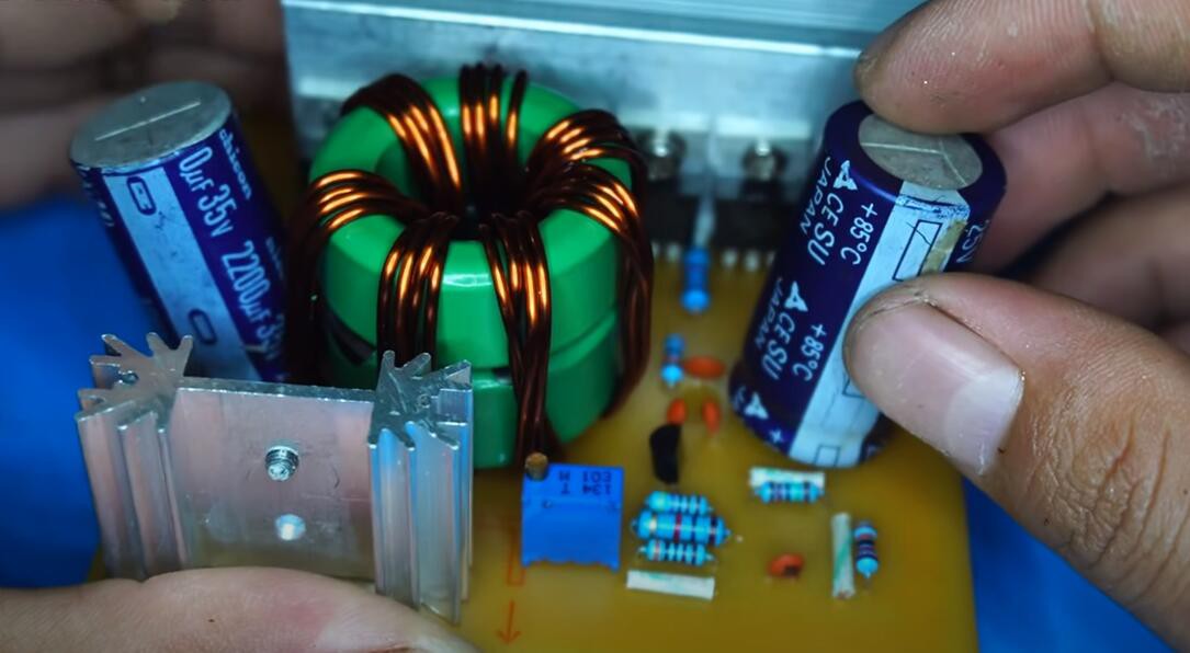
All the material you need for this project:

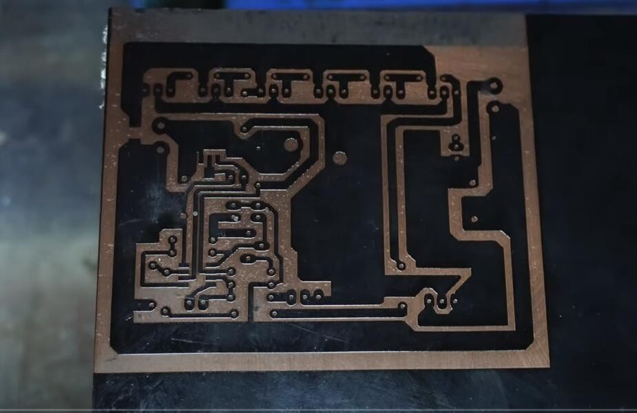
Here are the steps of this project:
1.

2.
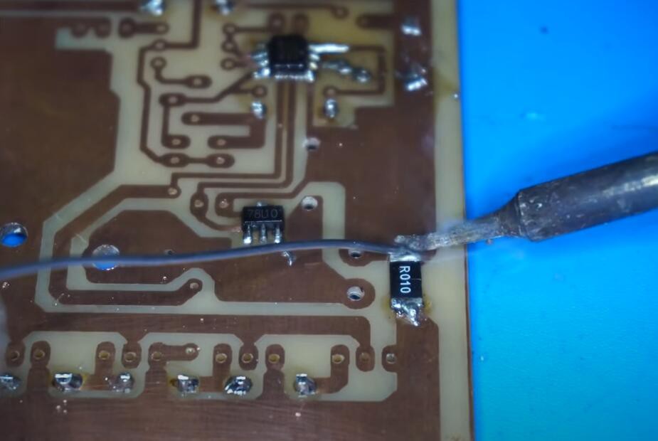
3.
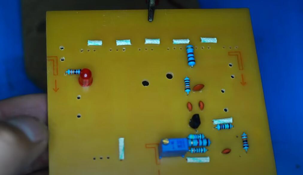
4.
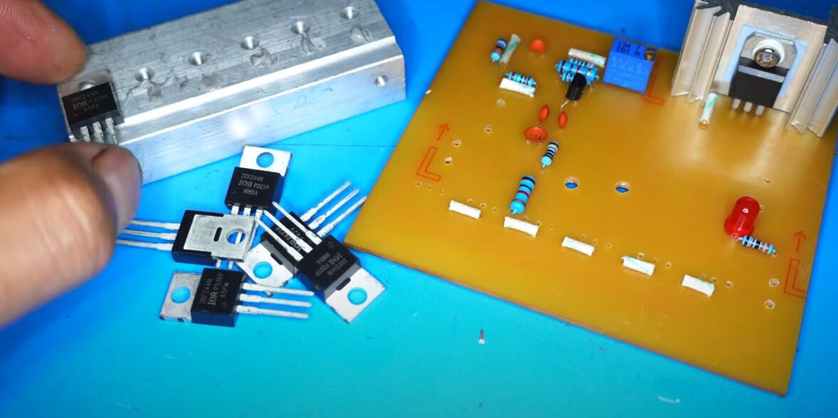
5.
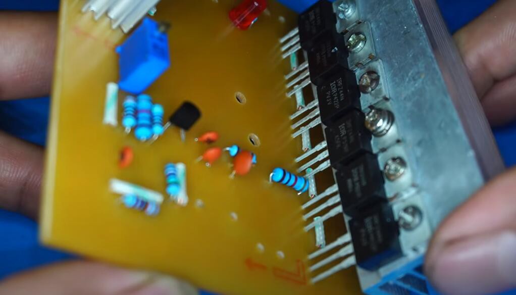
6.
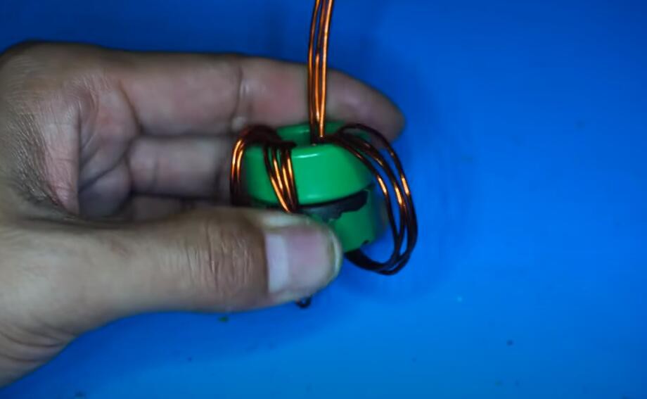
7.
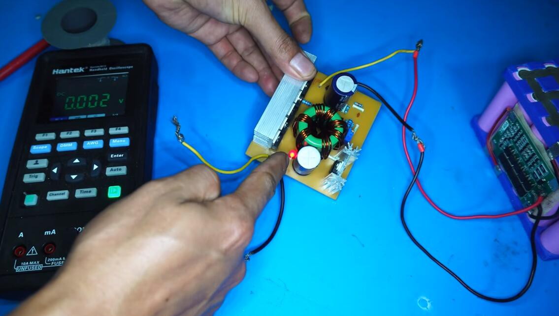
Show results:
The product links as below:
IC chips: https://www.utsource.net/category/ele...
Modules: https://www.utsource.net/Modules?sour...
Passive components: https://www.utsource.net/PassiveDevic...
Sensors: https://www.utsource.net/home/sensors...
LED lightings: https://www.utsource.net/category/led...
More electronic components you may be interested:
VIPER22A https://www.utsource.net/itm/p/11226780.html
Product Attributes
Not found, similar datasheet recommended
Description
The VIPer22A combines a dedicated current mode PWM controller with a high voltage Power MOSFET on the same silicon chip. Typical applications cover off line power supplies for battery charger adapters, standby power supplies for TV or monitors, auxiliary supplies for motor control, etc.
Features
● FIXED 60 KHZ SWITCHING FREQUENCY
● 9V TO 38V WIDE RANGE VDD VOLTAGE
● CURRENT MODE CONTROL
● AUXILIARY UNDERVOLTAGE LOCKOUT WITH HYSTERESIS
● HIGH VOLTAGE START UP CURRENT SOURCE
● OVERTEMPERATURE, OVERCURRENT AND OVERVOLTAGE PROTECTION WITH AUTORESTART
IR2110 https://www.utsource.net/itm/p/11537319.html
Product Attributes
The IR2110/IR2113 are high voltage, high speed power MOSFET and IGBT drivers with independent high and low side referenced output channels. Proprietary HVIC and latch immune CMOS technologies enable ruggedized monolithic construction. Logic inputs are compatible with
standard CMOS or LSTTL output, down to 3.3V logic. The output drivers feature a high pulse current buffer stage designed for minimum driver cross-conduction. Propagation delays are matched to simplify use in high frequency applications. The floating channel can be used to drive an N-channel power MOSFET or IGBT in the high side configuration which operates up to 500 or 600 volts.
Features
● Floating channel designed for bootstrap operation Fully operational to +500V or +600V Tolerant to negative transient
voltage dV/dt immune
● Gate drive supply range from 10 to 20V
● Undervoltage lockout for both channels
● 3.3V logic compatible Separate logic supply range from 3.3V to 20V Logic and power ground ±5V offset
● CMOS Schmitt-triggered inputs with pull-down
● Cycle by cycle edge-triggered shutdown logic
● Matched propagation delay for both channels
● Outputs in phase with inputs
What is IR2110
IR2110 is a MOSFET gate driver IC that can used to drive high and low side configurations. Usually to drive two MOSFETs in half bridge or high and low side configuration we will need complicated driver circuit with complementary transistors dual voltage supplies and lots of other complementary devices such as resistors, capacitors and diodes. However, we can achieve the same function using IR2110 MOSFET driver IC only using few other complementary components. You can see the physical appearance of the IR2110 MOSFET driver IC in below image.
Pinout of IR2110:
IR2110 MOSFET driver IC comes in a 14 pin DIP package and a 16 pin SOIC package. In below image pinout of the 14 pin DIP packaged IR2110 IC is given.
SupplierFile/202005/19/f_4d183d72de624310bc79add094367663.png
Figure 3. – Pinout of IR2110
Lets identify the pin functions and more details on each pin of IR2110
· Pin 1 – LO – Low side MOSFET gate output pin
· Pin 2 – COM – Low side return pin or the MOSFET common pin.
· Pin 3 – VCC– Voltage supply for the gate voltage.
· Pin 4 – NC – Not connected
· Pin 5 – VS – High side floating voltage supply return pin
· Pin 6 – VB – High side floating voltage supply pin
· Pin 7 – HO – High side MOSFET gate output pin
· Pin 8 – NC – Not connected
· Pin 9 – VDD – IC control power input
· Pin 10 – HIN – High side driving signal input
· Pin 11 – SD – IC shutdown input
· Pin 12 – LIN – Low side input signal
· Pin 13 – VSS – Ground connection
· Pin 14 – NC – Not connected
Features of S202S02:
Lets identify the key features of the IR2110 MOSFET driver IC
· Up to 600V driving voltage
· 10V to 20V gate drive capabilities
· 3.3V minimum logic supply voltage.
Basic Circuit Diagram:
Given below is the basic circuit diagram of the DIY cooler/ Heater circuit.
SupplierFile/202005/19/f_cf8702025d654317b86314b29f4d0b60.png
Figure 4. – DIY cooler / Heater
Key Components :
We will need fallowing components other than our key components. Each and every component is given below in the list
1. IRFB4227 MOSFET
2. IR2110 MOSFET Driver
3. 1N4001 diode
4. 2.2kΩ resistor
5. 0.22nF capacitor
6. 4.7uF 100V capacitor
7. 1uF capacitor
Tools Needed:
1. Soldering Iron
2. Iron Stand
3. Flux
4. Nose pliers
Step By Step Guide:
Step 1: Arrange above given components.
Step 2: Solder or connect all the components as shown in the circuit diagram.
Step 3: Supply all three supply voltages. You adjust the 5V and 48V as per your requirement
Step 4: Connect a pwm controller or an Arduino to the signal inputs.
How It Works:
When the control signals are provided IR2110 will drive the two MOSFETs according to the signal you can change the polarity and change the effect to cooling or the heating.
Conclusion:
This can be used as a room cooler or heater with proper insulation. And this also can be used as a CPU cooler pith proper setup with fans.
TDA7388 https://www.utsource.net/itm/p/11266210.html
Product Attributes
Introduce this Module:
The TDA7388 is an AB class audio power amplifier, packaged in Flexid 25 watt, and designed for high-end car applications.
Based on a fully complementary PNP/NPN Transistor configuration, the TDA7388 allows a rail to rail output voltage swing with no need of bootstrap capacitors. The extremely reduced boundary components counter allows very compact sets.
Some Core Parameters of the Module:
SPECIAL FEATURES :
● High output power capability: 4x45W/4 Ohm max.
● Low distortion.
● Low output noise.
● Standby function.
● Mute function.
● Automate at min. supply voltage detection.
● Internally fixed gain (26dB).
How it Uses in the work:
Internal Block Diagram:
SupplierFile/202006/23/f_d5a574b9425a4cca91409876f1d0a1c3.png
TDA7388 Pinout Connections:
SupplierFile/202006/23/f_83e845858fa04133a631d2ef6487e52b.png
TDA7388 Pin Functions:
● VS - Operating supply voltage 18V.
● VS(DC) - DC supply voltage: 28V.
● VS(pk) – Peak power supply voltage (time = 50ms) 50V
● I(O) - Output peak current: Repetitive (duty cycle 10 % at f = 10 Hz) Non repetitive (t = 100μs) 4.5A.
● P(tot) - Power dissipation, (Tcase = 70℃)
● TJ - Junction temperature 150℃
MN3101 https://www.utsource.net/itm/p/305474.html
Product Attributes
MN3101 Description
The MN3101 is a complementary metal-oxide-semiconductor (CMOS) which generates a two-phase clock signal of low output impedance for driving MN3000 series BBD. The Built-in VGG power supply circuit for the MN3000 series BBD* is most suitable VGG voltage for the BBD when the MN3101 is used with the same power source as BBD.
The Oscillation is controlled properly via external resistors and capacitors and also oscillation can be controlled via separate excitation. The Clock signal frequency is the 1/2 of oscillation frequency.
The Pin-out diagram of MN3101 IC is given below.
SupplierFile/202006/05/f_a572944c2d9545268d1fa6b631e6d5c7.png
Fig 1 : Pin Description of MN3101 IC
Specifications and Features of MN3101
1. BBD is capable of driving up to two MN3005s (equivalent to 8192 stages) which gives it more important than others.
2. It provides a two-phase clock output (Duty 112).
3. There is a built-in VQG voltage generator for the BBD.
4. Single Power Supply 8~16 V is provided .
5. There is an 8-Lead Dual-in-Line Plastic Package for the IC.
Working Principle of MN3101
In CMOS logic gates a collection of n-type MOSFETs is arranged in a network between which is pull-down the output and the low voltage power supply rail (Vss or quite often ground). Instead of the load resistor of NMOS logic gates, CMOS logic gates have a collection of p-type MOSFETs in a pull-up network between the output and the higher-voltage rail (often named Vdd) and it provides additional protection as shown in the figure below.
SupplierFile/202006/05/f_7fac5da0b2914ebe964ce8852d3e1bb8.png
Fig 2 : Schematic of a CMOS
1. It is mainly used as BBD Clock Generator/Driver
2. It is also used as the oscillation generation circuit also.
SupplierFile/202006/05/f_89abebf19f9a4a8182e2b620a5285a34.png
3. It used for providing Reverbation effect in audio consoles and microphone.
4. It is used as fixed or variable delays in Analog signals
5. Telephonic line compression and delay can also be done by using this MN3101.
Mainly this particular type of CMOS is used for the Time delay mechanism in the clock pulse driven circuits, also we can use this Registrars, Latch, Flip-flops for the time delay mechanism purpose. In digital design, this has a very wide range of applications.
IRF840 https://www.utsource.net/itm/p/11228186.html
Product Attributes
Description
These TMOS Power FETs are designed for high voltage. high speed power switching applications such as switching regulator. Converters solienoid and relay drivers.
Features
● Sillicon Gate or Fest Switching Speeds
● Low to Minimize On-Losses Specified at Elevated Temperature
● Rugged - SOA Is Power Dissipation Limited
● Source-to-Drain Diode Characterized for Use With Inductive Loads
For more details, pls check the video on youtube: