 Aldwin
Motivation
This projects goal is mainly to see how far I can build/design a device from scratch ( previous attempt here and here )
In my spare time I always love to build something, but most of the time it's never completed ( i.e. here ) as I've always aim it too complex. This time is different, I set the MVP low and simple and most importantly aim to just finish the project in short amount of time. Hence, why there are some questionable design that I took or that does not follow the recommended manufacturer application. Listed below are some notes on the design:
- On-board Antenna does not follow manufacturer suggestion. There should be more empty ground plane below the antenna.
- It is possible to just use the u.fl connection from the RAK3172 module, that way radio performance can be improved
- NanoVNA can be used to further tune the on-board antenna
- Air flow to the BME680 is probably not the best. Maybe adding few vents in the case is better? or move the sensor more further towards the edge and away from other components?
Let me know if there's any questionable design, would love to learn more!
Specification
- RAK3172: An STM32WLE5CC module
- AEM10941: Solar energy harvesting
- 3.3V only power/pin.
- 3uA Deep-Sleep
- BME688 for Environmental Sensing
- Switchable TX Power. 14 dBm(50mA) or 22 dBm(140mA) ( on 915MHz frequency )
- Supports LoRaWAN 1.0.3
- ~1KM Range
- UART2 breakout for Arduino progamming
- SWD breakout for Mbed OS/STM32Cube programming
- IPEX antenna connector
- 3.7 Volts LiPo Battery
Schematics

Boards

Built using KiCAD, the board is design to be as small as possible with all components placed on the top side of the PCB. The following are the lists of revision of the board:
- Revision 1: Initial design
- Revision 2: Better trace, use rounded trace and change solar cell wiring to parallel for all cell
- Revision 3: Rename 3V3 to PRIMIN and breaks out PRIMIN
The following design are based on the latest revision.
| Top Board | Bottom Board |
|---|---|
|
|
|
|


Case

Built using TinkerCAD, the cases are available with 2 variant, with or without the programming port. The cases are 3D printable with any generic 3D printer with/without suppport (depends on the orientation). The STL files are available here

The case is design to be as small as possible with an additional magnets in the back to ease the placement of the sensor. The following are the list of material used at the time of testing:
- 3.7v LiPo Battery, 400 mAh 50mm x 25mm x 35mm ( it is possible to use 2 of this in parallel )
- 4 piece of 8mm x 2mm neodymium magnet

Sensor Placement with Magnet
Measurement
Power consumption and solar charging current are measured using Nordic PPK2 and CurrentRanger. The following are the summary of the measurement:
- Transmit 14dBm: 305ms @ 20mA
- Deep-Sleep : 3.22 uA
- Direct Sunlight Solar Charge: 9mA
- Indirect Sunlight Solar Charge: 300uA


| Solar Charge - Direct Sunlight | Solar Charge - Indirect Sunlight |
|---|---|
|
|


More measurement can be found here
Programming
Board can only be powered using the LiPo Battery
Programming the device can be done over the UART2 or SWD, available on the right side of the board. Out of the factory, the RAK3172 chip ships with an AT firmware that can be tested by connecting a USB-to-UART bridge to the UART2 port.
The following are some very good tutorial to start developing with the device:
- Communicating with the AT firmware
- Programming with Arduino
- Programming with STM32Cube
- Programming with MbedOS
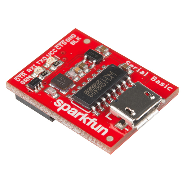
For connecting to the UART2 port, use any USB-to-UART bridge module. In testing, the Sparkfun board is used for communication with AT firmware and programming over Arduino.
Be sure to only use 3.3V module. Do not 5V module
For connecting to the SWD port, use ST-Link v2 in-circuit debugger and programmer from STM. In testing, ST-Link v2 clone will not work. The ST-Link v2 should atleast be reconizeable by the STM32CubeProgrammer. A cheap and alternative way to get an authorized ST-Link is to buy a Nucleo board, cut the top part which contain the ST-Link and use it as an external programmer.

Here are some good tutorial to convert a Nucleo to and external ST-Link v2:
- https://www.radioshuttle.de/en/turtle-en/nucleo-st-link-interface-en/
- https://jeelabs.org/book/1547a/index.html
Notes
There are some issue, notes, and behavior that was discovered at the time of testing and development. The following are those discovery:
- Soldering the solar cell is better to be done manually using a soldering iron. Without proper reflow oven, it may damage the solar cell and reduces it's efficiency
- Using Arduino RUI3 framework may introduce some-instability after programming. It is observed that by randomly power-cycling the board in-short interval after flashing, causes the board to hang in Boot mode
- PRIMIN ( or 3V3 in old revision ) is available to use as the input for AEM10941 Primary Battery input. See schematic for more detail
- PA15 or ADC5 in Arduino RUI3 is currently not working. This causes the battery measurement to not work as well. An alternative is to use Mbed OS.
Reference
The project won't be possible without the amazing work from people across the globe. The following are the reference to those awesome projects: