 Christoph
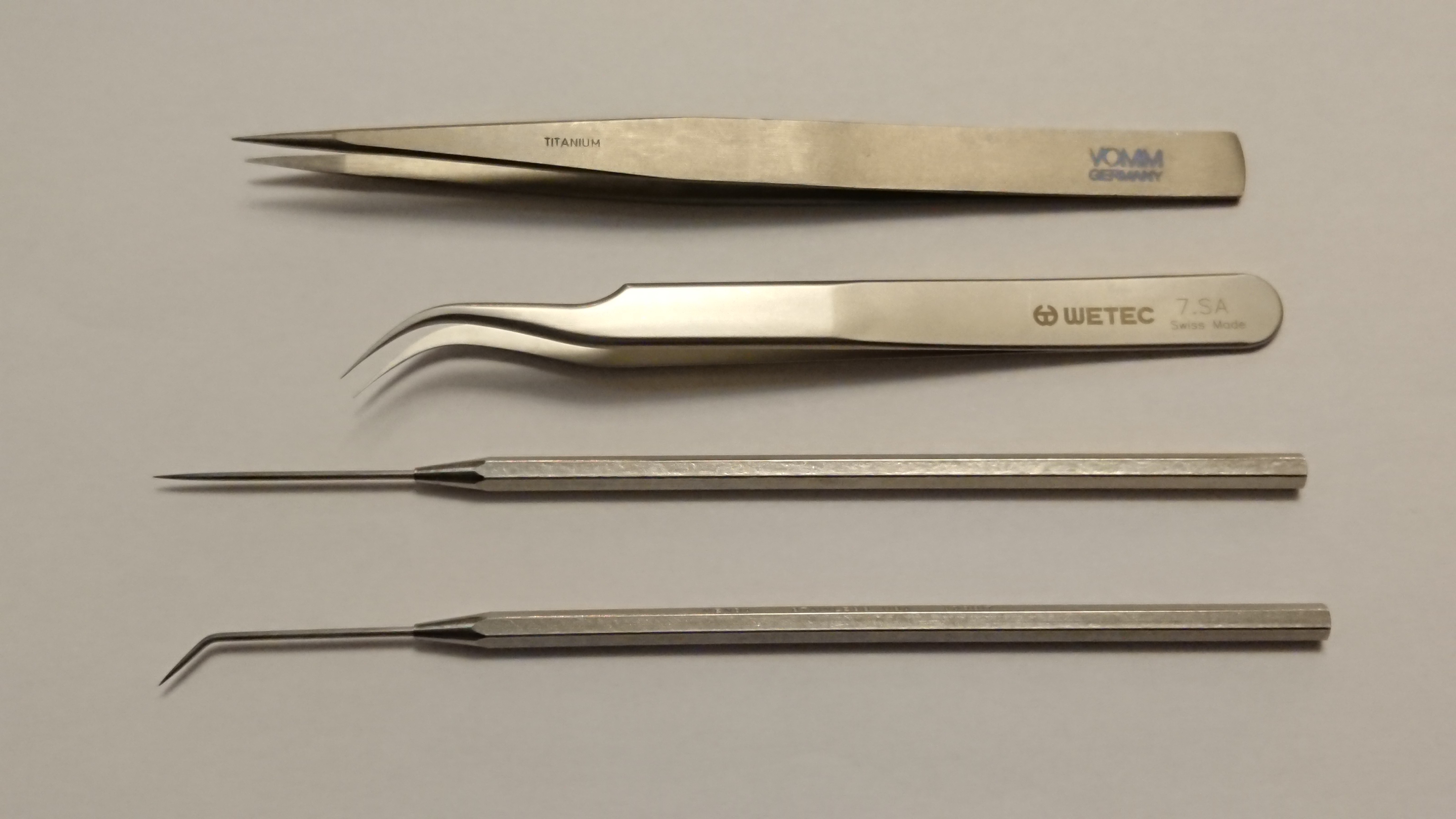
With appropriate visual feedback (= magnifying glasses or a stereo microscope) you can adjust a part's position by 0.1 to 0.05 mm. It takes patience and a bit of practice, but it's certainly doable. I use a stereo microscope with 10x magnification most of the time, good tweezers (to place parts) and those pointy dentist things (to poke parts):
Let's have a look at how that compares to the size of small passives. Here's KiCad's stock 0201 footprint with the corresponding 3D view:
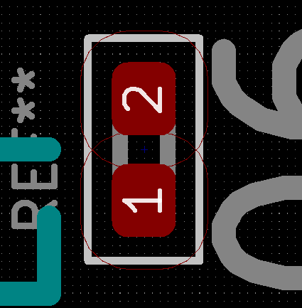
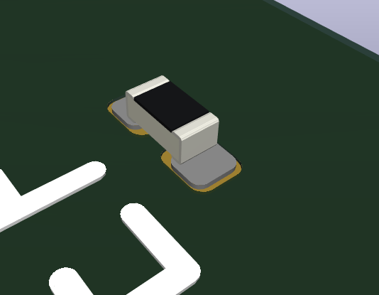
The pads are 0.46 mm wide. Let's offset the part a bit, say, 0.15 mm:
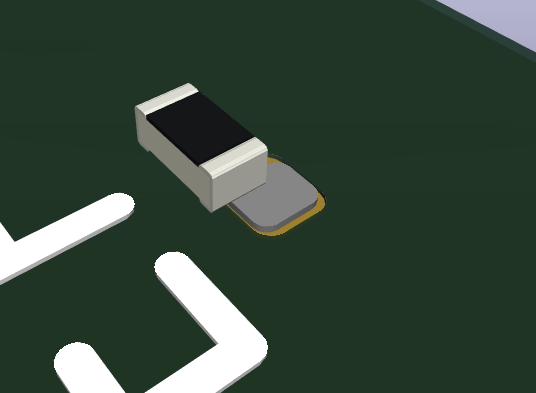
That's not going to ruin your PCB (unless it overlaps with other footprints), and you can easily give it a little nudge in the right direction so that it sits almost perfectly. The solder will pull it towards the pad's center and do the rest. Well, almost, because the stock footprint is too long. If one pad is already at reflow temperature and the other isn't, it might pull the part too far - like so:
and the part could tombstone. Let's fix that with a shorter footprint (I'll add it to the project files):
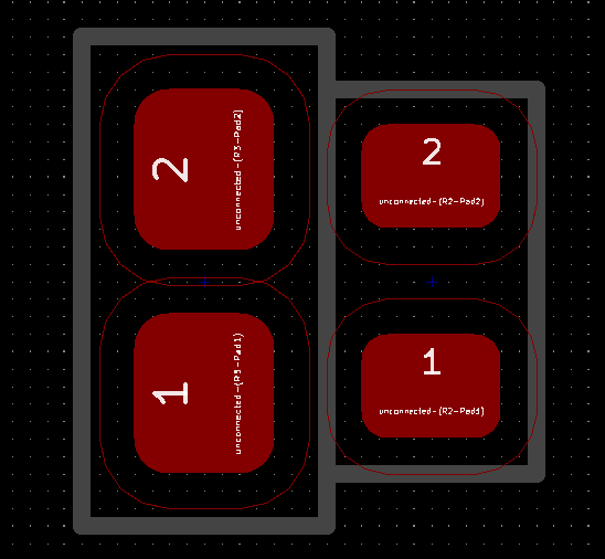
Left: stock KiCad footprint. Right: What I use (iirc it comes from some AVX datasheet or appnote). I use this very footprint in #Effect of moon phase on tombstoning and it has been pretty robust so far.
Not only does it not mess with you, there's one more benefit: The pad clearance areas don't overlap (assuming 0.1 mm spacing) and there's enough room to route a 0.1 mm trace between them:
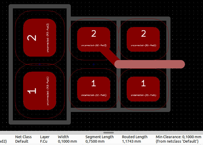
JLCPCB supports that width/spacing for 4 and 6 layer boards, so it's really not out of reach for hobbyists.
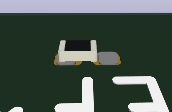
Let's also compare that with a larger QFN which might seem less intimidating than an 0201 resistor. Here are both next to each other, with the QFN (0.4 mm pitch) displaced by 0.1 mm:
If you have ever soldered a QFN, you've probably tried to correct such a displacement.
Bottom line: 0201s are not harder to place than large fine-pitch packages, and they'll behave alright with the right footprint.
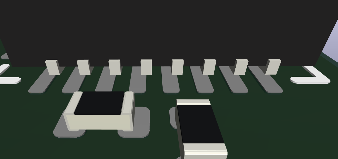
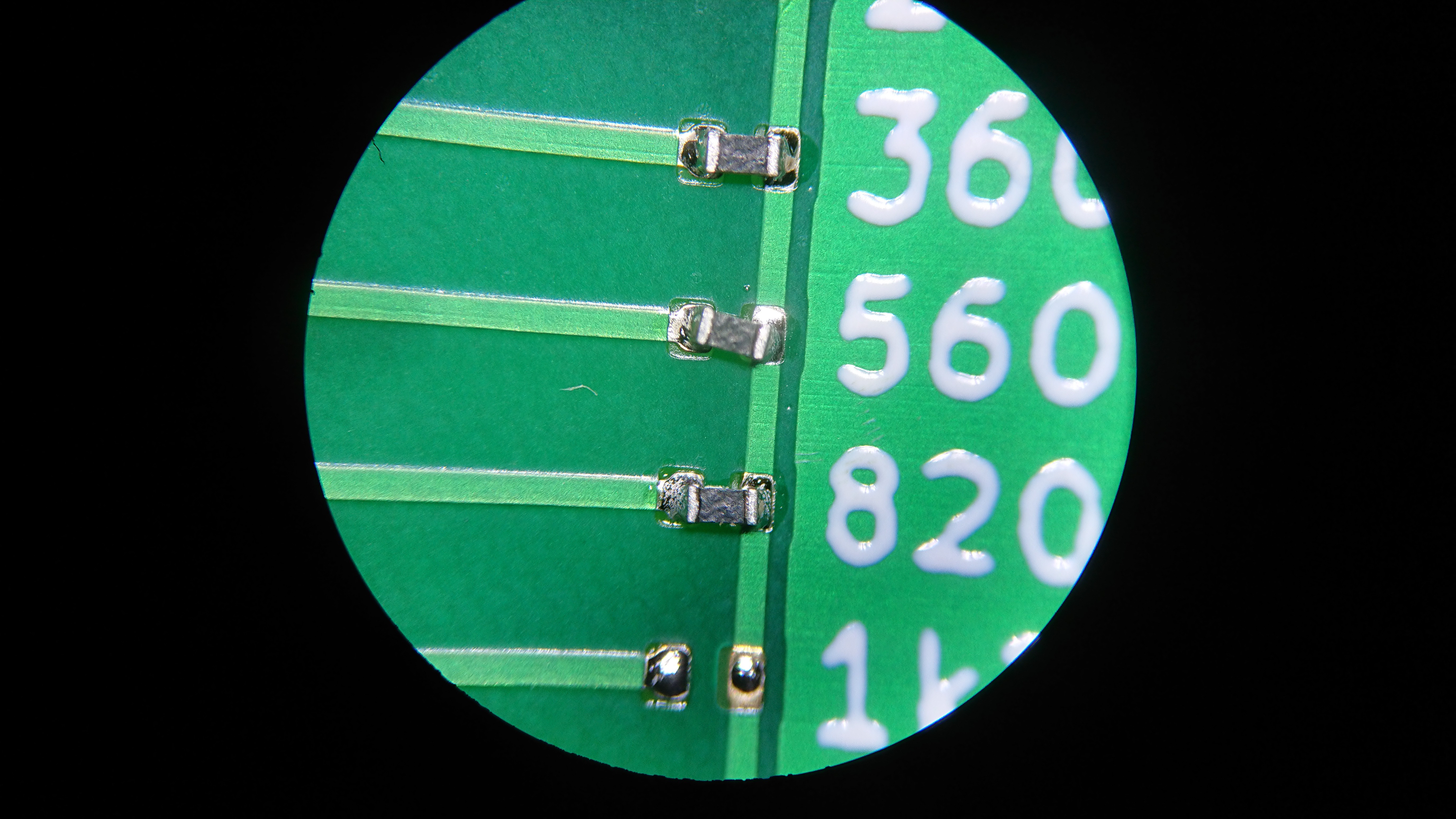
To demonstrate that we can get away with considerable displacement, here's a before and after reflow picture of three 0201 resistors I deliberately placed slightly off.
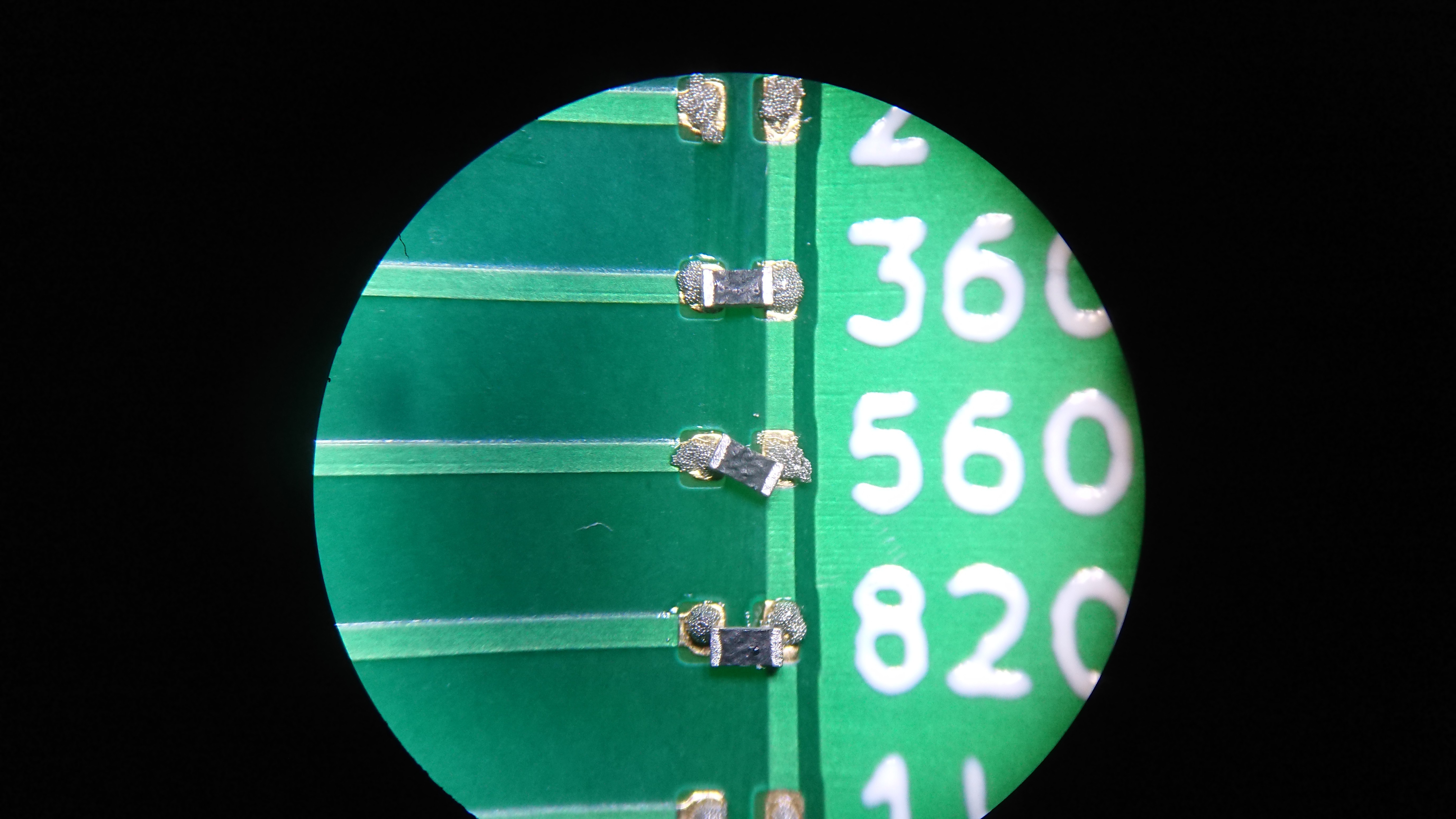
Microscope with 30x magnification.
top: placed slightly to the left. It's hard to see, but the resistor barely touches the pad on the right side.
middle: That's at an angle.
bottom: about 0.15 mm off both pads towards the bottom
This is how it turned out:
Discussions
Become a Hackaday.io Member
Create an account to leave a comment. Already have an account? Log In.