0%
0%
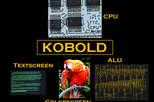
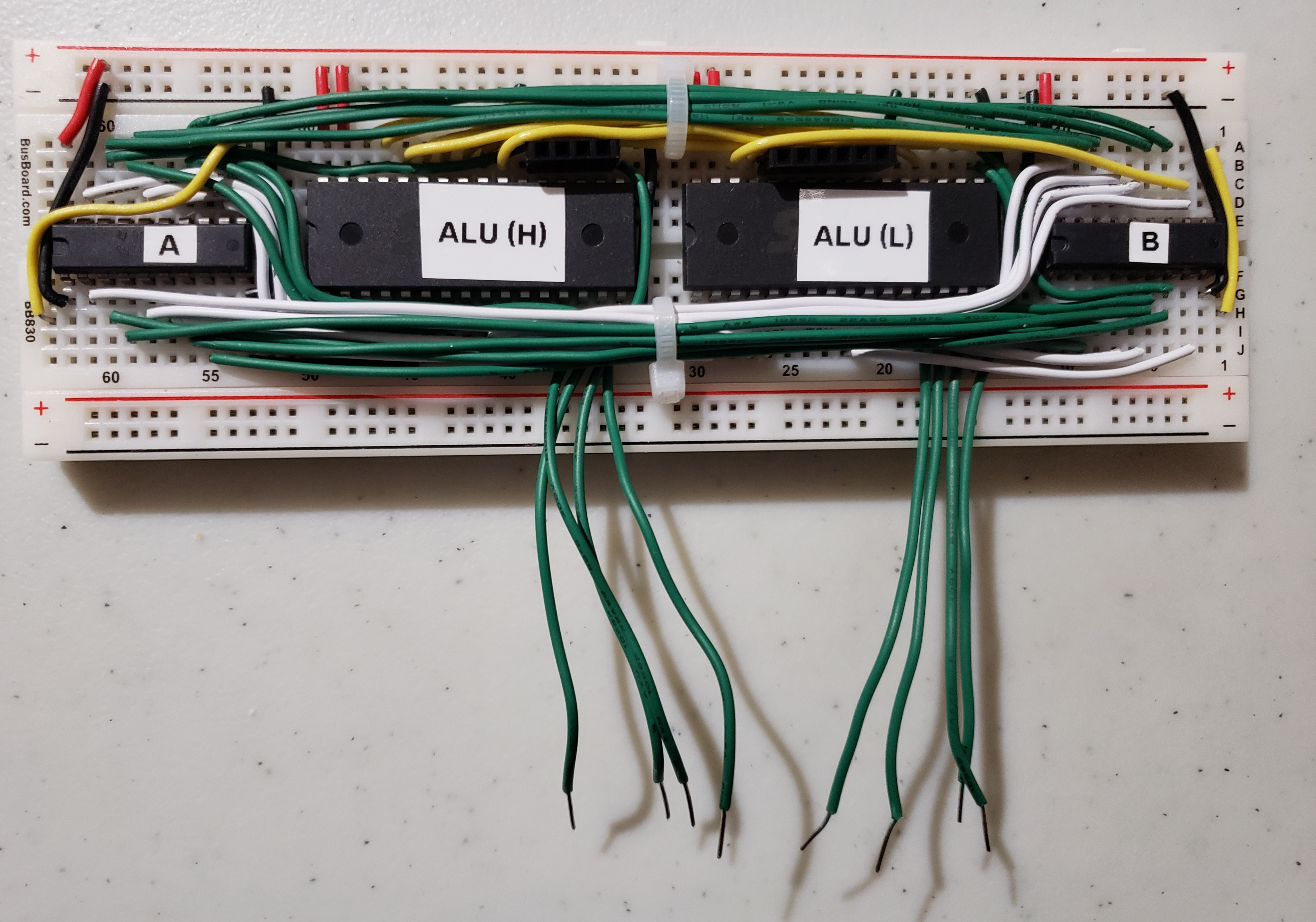
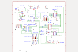
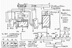
Flash 6502
Trying to build a 6502-compatible CPU on breadboards, using as few chips as possible.
 Patrick LeBoutillier
Become a Hackaday.io member
Already have an account? Log in.
Just one more thing
To make the experience fit your profile, pick a username and tell us what interests you.
Pick an awesome username
hackaday.io/
Your profile's URL: hackaday.io/username. Max 25 alphanumeric characters.
Pick a few interests
Projects that share your interests
People that share your interests
 zpekic
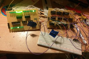
 Boxerbomb