 Alan
AlanPOE(Power Over Ethernet)
- It refers to power transmission technology itself, and its components are divided into PSE and PD.
- It is a technology that can transmit power and data to devices over Ethernet using Cat 5 twisted-pair cables.
- It can operate without having to change the Ethernet cable structure, saving time and money for cable configuration.
- It has remote power on/off, short circuit protection, over-voltage/low voltage protection, and over-current protection
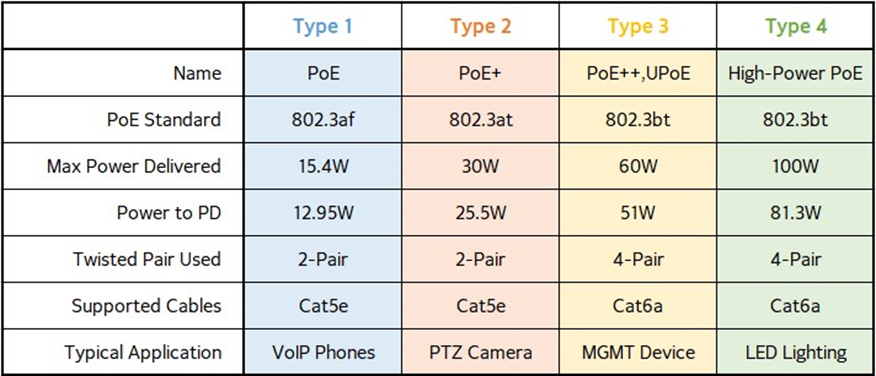
The PoE international standard is divided into IEEE 802.3af/802.3at/802.3bt. As shown below, it is divided into four types depending on the amount of power, and you can select and use it according to the application you use.
PSE(Power Sourcing Equipment)
- Power the Ethernet cable and manage the power.
It is divided into two types, Endspan and Midspan, depending on the power transmission method. There are usually many PSE devices that support only one, and there are few PSEs that support both, but the price is high.
Endspan PSE (Mode A)
- It is a method of delivering electricity through a data line. Power is transmitted to CT of PSE and received to CT of PD.
- As a disadvantage, the implementation is relatively complicated, and since power is supplied to the data line, it may be vulnerable to power noise.
- The advantage is that it can also be used at 1000 Mbit, and it can be combined with Mode B to satisfy higher power transmission specifications.
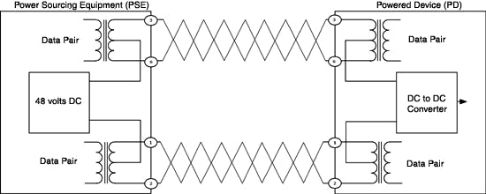
Endspan PSE (Mode A)
Midspan PSE (Mode B)
- Since only two pairs (1, 2/3, 6) are used for data transmission in the 802.3af standard, it is a method of transmitting power through wires 4, 5/7, 8 that are not used for data transmission.
- It is typically used on 10/100 Mbps equipment that supports only the 802.3af standard.
- Simple to implement, low cost.
- There is stability
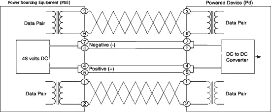
Midspan PSE (Mode B)
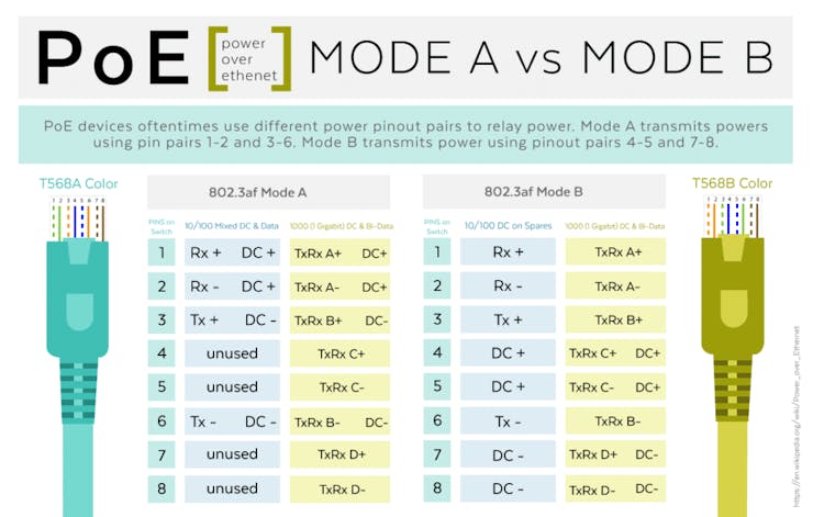
Endspan vs Midspan Since the lines used are different, cables are also divided.It is divided into T568A and T568B.
<VERSA Technology>
PD
It is a device that receives power and uses it. Examples include IP phones, IP cameras, and PDAs.
It is now the beginning of full-fledged development.
The goal
The goal is to create a PD module that is compatible with both Mode A and Mode B. PD needs to receive about 48V from PSE and produce an output voltage of 5V. However, the PSE does not vaguely output 48V. PSE sends out the output through its own process.
PoE Process
<AAEON Forum>
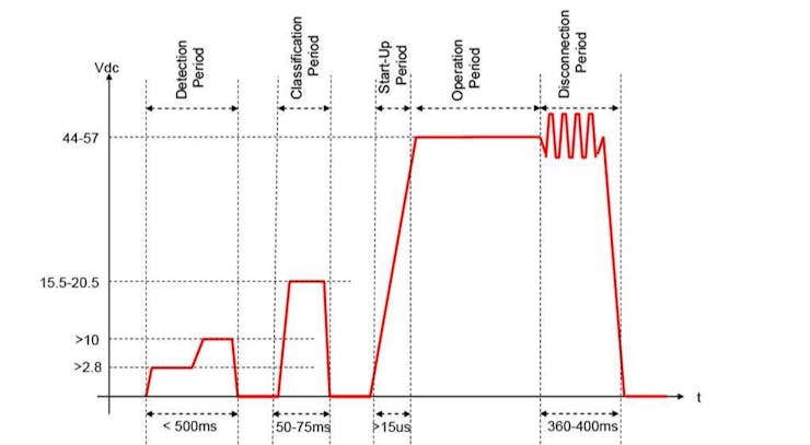
1. Detection Period
The PSE equipment outputs a very small voltage from the terminal until it detects that a PD supporting the IEEE 802.3af standard is connected to the end of the cable.
<AAEON Forum>
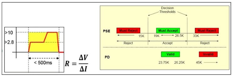
Continue to release 2.8V and 10V at 500ms intervals (until PD is detected). Then, the resistance value of PD is measured by calculating the current. When the resistance value falls within the category of about 25k, it moves on to the next step.
2. Classification Period
When a PD is detected, the PSE evaluates and classifies how much power the PD consumes.
3. Start-up Period
The voltage rises to 44-57 V in less than about 15 us.
4. Operation Period
It is a stable period of operation.
5. Disconnection Period
When the PD connection is disconnected, the PSE repeats "1. Detection Period" again.
This is a real development : )
Looking at the PoE process in this way, it seems that power will be output normally if only 1.2 is well accommodated.
The PSE device to be used for development is the EDIMAX 8Port device shown below. Only Mode B is supported.
EDIMAX 8Port PSE Device
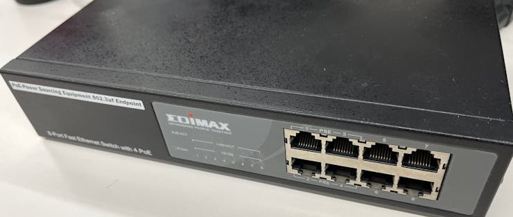
<EDIMAX 8Port PSE Device>

https://maker.wiznet.io/mason/projects/duino-coin-mining-with-wiznet-w5100s-pico-mining-rig/
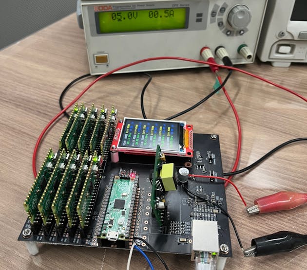
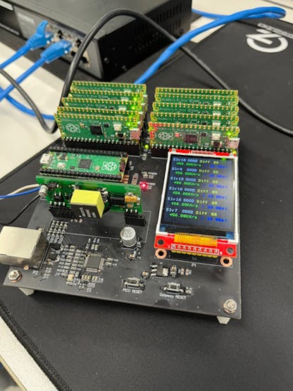
The device to be used as a PD is the Mining board. A PD module to be provided by converting the on voltage from the PSE will be made, so a PD to receive and use the voltage is needed. The board is equipped with Silvertel's Ag9700 module. We are planning to remove this module and design it on the spot.
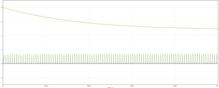
First, I put 24.9k resistance on the output terminal and took a voltage.
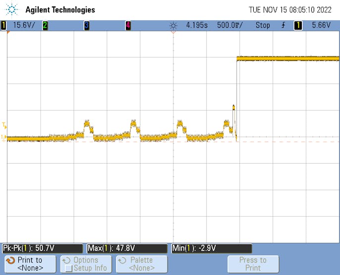
It was shown by the above waveform above. The process seems to be working normally.
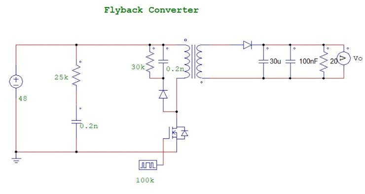
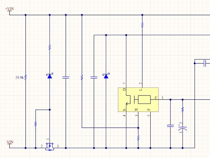
<Flyback Circuit Diagram Implemented by Psim>
<Psim Action Implementation>
The circuit to implement is likely to be Flyback anyway. Basically, I turned Flyback with Psim and implemented it as it is, but since the output is not fixed at 48V, it is natural that the output will change depending on the input if the PWM is fixed to the switch.So, it has to adjust the input duty by receiving feedback.
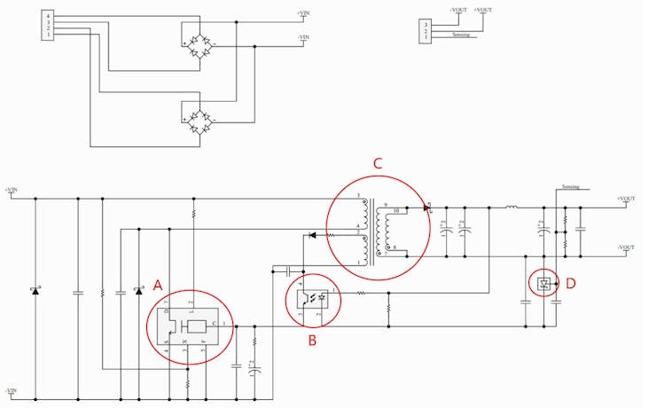
The circuit was constructed as above.
- A: There are many different chips and many applications for Flyback just by searching Google. I used the kindest one of them. It is an FET that receives a feedback signal and controls Duty.
- B: It's a popular Photocoupler. It must be installed for insolation, and the more precise the operation is desired, the faster the operation can be selected.
- C: One of the Transformers for PoE was selected. It was selected as 1:0.5:0.5:0.5, and the final test result seems to be good enough. But it's a bit pricey
- D : A diode that has its own reference voltage and is surrendered when the input reference exceeds that value.I can just use the Zener diode of the desired voltage, but this part is much more delicate and accurate than a regular Zener.
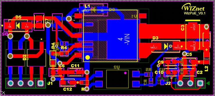
<Artwork appearance / named WizPoE_V0.1>
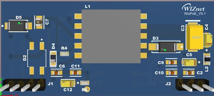
The artwork has been completed as above. 3D doesn't have many libraries, so it looks weird... But I don't want to add it because I'm lazy
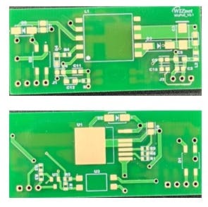
<BarePCB>
After 3 nights and 4 days, I was able to get a PCB. In the meantime, materials have also been received.
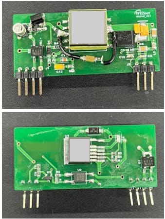
Actually, I've already finished the experiment so much that I've already touched the board a lot.
Start a motion experiment
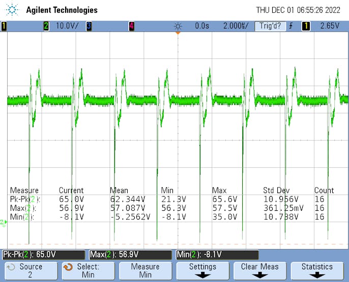
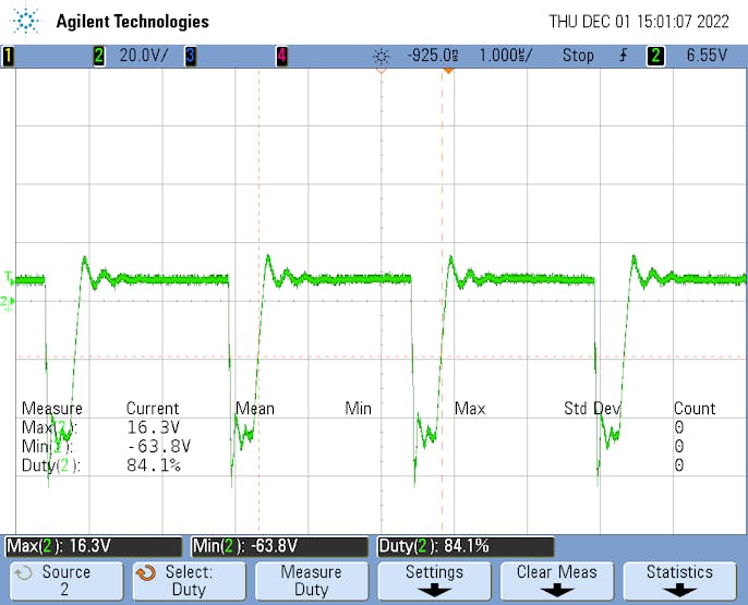
The problem arose from the outset. I thought that once only 48V was output, I could somehow adjust it and output 5V, but when I made the first operation after assembly, the output waveform was shown as follows.
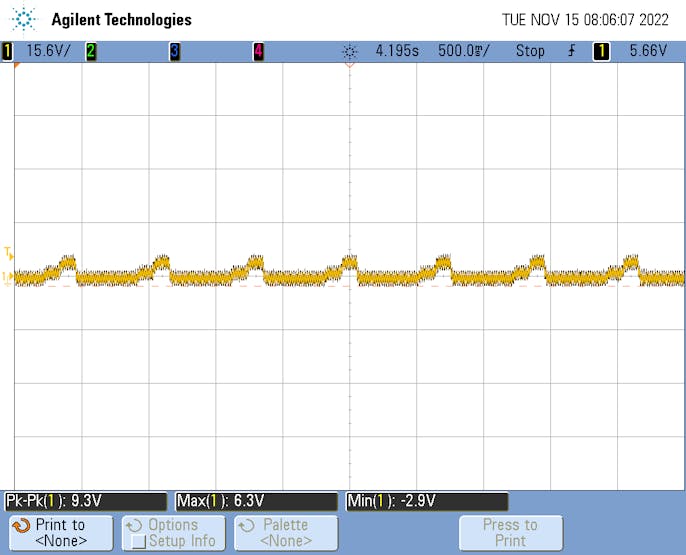
<Oh.....;; PSE is looking for a PD over and over again.>
PSE is continuously looking for a PD.As experimented above, when only 24.9k was attached, 48V was immediately output, but unlike then, PES continued to look for a PD.It didn't take 24.9k because the input/output was short through L.It was because I didn't study much about PoE and only watched Flyback carefully.
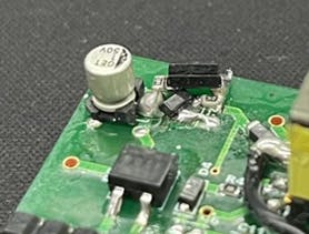
So I decided to use the switching element. I decided to use the 2N7002 N-Channel MOSFET I had. 24.9k is installed at the input terminal and FET is installed at the VIN- terminal, so that the PSE recognizes 24.9k and the FET can be turned on as soon as the voltage rises. (Picture above)The Zener diode used its 12V one and configured a voltage divider resistance according to the FET Gate voltage level.
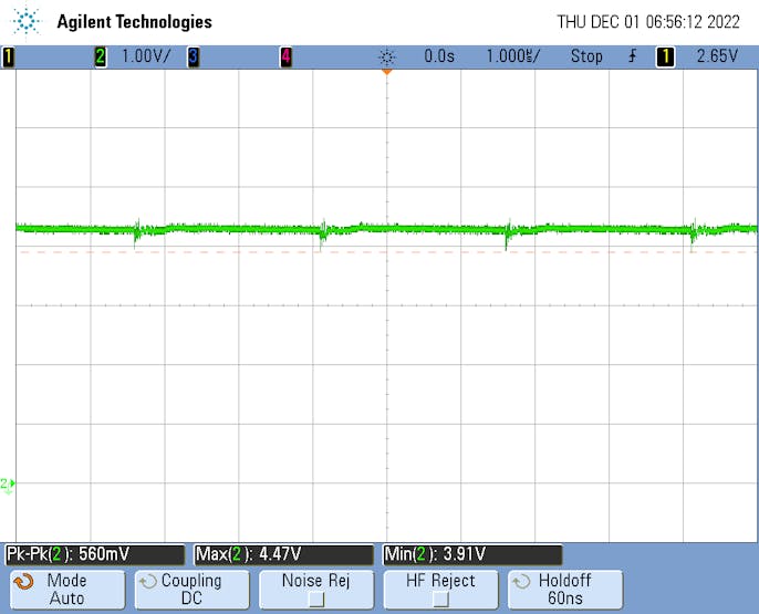
The 48V output comes out at a glance, but the voltage does not appear normally. When both ends of the input are measured, there is a tremendous amount of noise. Considering that the frequency is about 500k, it seems to be a switching frequency. Perhaps the cap component is small, so it seems that it cannot withstand the current being pulled toward the output during switching.
So I installed a slightly larger Capacitor. It's a little bigger than the spec, but there's nothing suitable now, so I put it on for now. The 48V is output very neatly.
The output is approximately 4.2 volts...Why...?
Both ends of the drain-source of the switching element were measured... Duty is about 15 per cent. It's still a long way off before it's saturated. When I took a feedback signal, the output was less than 5V, but the feedback signal kept coming in.
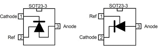
It turned out to be an Artwork miss for the Voltage Reference element. In the picture above, I designed it to the left, but it was on the right. Cathode and Reference were changed and installed, making strange movements.5V comes out well when installed normally.
Now it's time for a test.
Looking at the load of the Mining board to be tested, it takes about 0.5A. Approximately 2.5WIt should be about 15W to satisfy 802.3af. However, there is currently no device to give that much load.
Still, I'm going to make a load jig after the test at this level and make an Aging.
Discussions
Become a Hackaday.io Member
Create an account to leave a comment. Already have an account? Log In.