 agp.cooper
PCB Assembly
I have started assembly of the PCBs but I am waiting on a part.
Instruction Set
I have had time to think about improving the instruction set.
The idea came from the number of steps required to swap out the accumulator to memory. Better if I have a register and a swap opcode.
The idea actually frees up the opcode space as I can use the opcode "data" to specify the register and the registers can serve other purposes (e.g. the page register).
I need to look at how the memory data flow works as well.
Rebuilding the Micro-Architecture
I took the well published academic RISC micro-architecture:

And derived the CHUMP micro-architecture:
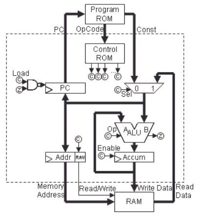
But along the way I saw an alternative memory arrangement:
This configuration has three benefits:
- The SRAM write logic is simplified (perhaps I over designed the write logic in the first place).
- The opcode logic is unchanged.
- The accumulator data can be written to SRAM in the same instruction cycle (CHUMP does it on the next instruction cycle).
I have tested the new micro-architecture in Logic-Sim (and it works fine.
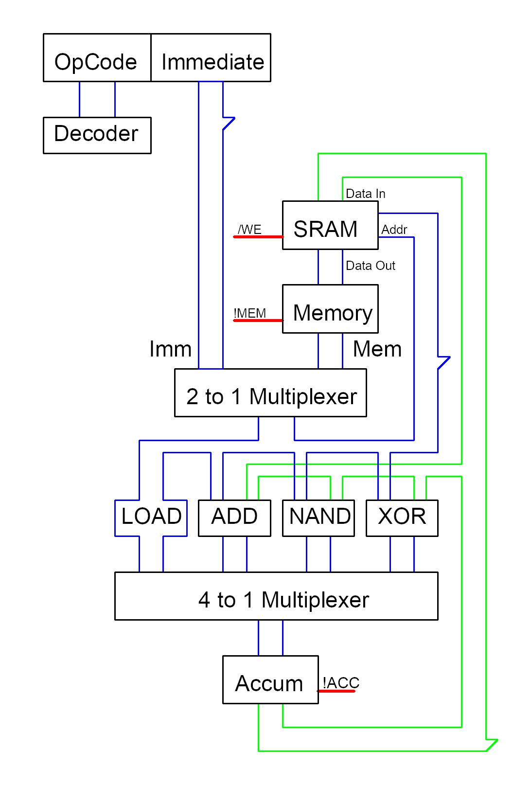
Adding Registers to the CPU
This allows the inclusion of register read/write logic:

In the above drawing I will probably keep the old PC and JNC logic.
Now I can replace the Page opcode with a register(s) read/write opcode.
Working LogiSim Version 7
Have been working on the Version 7, it now has register read/write opcodes. Added four registers of the eight available slots:
- Write Page/(no page read)
- Write Output/Read Input
- Write Reg A/Read Reg A
- Write Reg B/Read Reg B
Swapped the Page opcodes (Ex/Fx) with JNC opcodes (8x/9x).
Replaced the new 8x/9x opcodes with 8r/9r were r is a register constant or memory reference:
- Page: W/X = 0/4
- I/O: W/R = 1/5
- Reg A: W/R = 2/6
- Page: W/R = 3/7
Here is the Top Level:

The Control Unit:
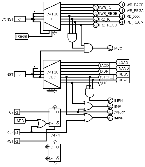
The ALU:

And the PC:

Overall a pretty significant improvements on CHUMP V5 and the 4 Bit CPU V6.
Here is the test code (the multiply algorithm):
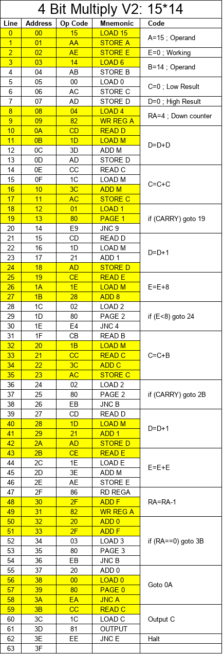
This algorithm uses the new JNC and REGs opcodes, and multiplies F x E (13 x 14), the result is D2 (210).
Parts have Arrived
The parts have arrived. Finished off one of the Diode ROM boards, next is the CPU board:

TBC ...
AlanX
Discussions
Become a Hackaday.io Member
Create an account to leave a comment. Already have an account? Log In.