 Eric Hertz
If you've read the last logs, you'll know I've been caught-up in trying to meet the 8088's bus-timing, using an AVR.
I think I went way overboard.
In one of the later logs on the matter I realized: It's not that I need to meet the 8088's *output* timing-specs, but that I need to meet the *input* timing-specs of the devices attached to it.
That certainly lowered the requirements on my AVR, but I still visualized a lot to be done within specific timings... Including (and probably most-difficult) setting up 20 address-bits, the S2:0 signals, and the QS1:0 signals, all within a single bus-cycle (at 4.77MHz). 25 bits to setup within one bus-cycle would, if set-up prior to the bus-cycle, require my AVR to be running 4x faster than the bus (writing one byte at a time).
Maybe, prior to that bus-cycle, I could've set up a timer output to toggle one pin within that cycle. Thus, not requiring an explicit instruction to be executed within that cycle to change that pin within that cycle... that'd bring the bit-count down to 24, three bytes would still require the AVR to be running at least 3x faster than the bus.
-----------
Tonight an epiphany.
If the bus is *idle* then it shouldn't matter what happens on the majority of the signals.
In other words: imagine an SRAM whose Chip-Select is disabled... It doesn't care what happens on the address lines.
Similarly, even if Chip-Select is enabled, changing the address lines willy-nilly doesn't affect the functionality of the SRAM until /RD or /WR is activated...
So, for all the SRAM ('device') cares, I could've set-up the address lines *hours* before-hand, if I wanted to.
The same could, likely, be said for most (maybe all) chips connected to the 8088's bus.
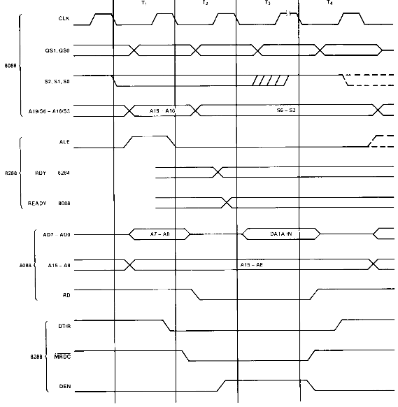
Right now I'm looking at the 8288, which, essentially, converts the 8088's multiplexed /S0-/S2 signals into various /RD and /WR signals...
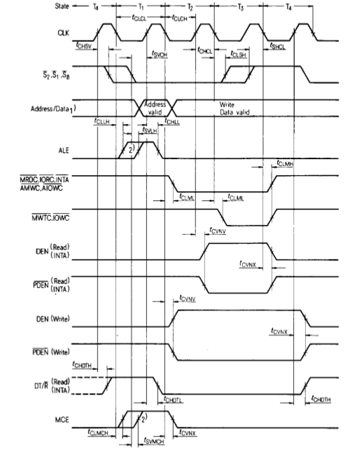
Basically, the vast-majority of 'devices'--be they on the ISA slots or on the mother-board--only receive their /RD, or /WR signals *through* the 8288. So, for those devices, as long as I meet the 8288's requirements, everything should go smoothly.
And, that's what I was missing, somehow, before...
I haven't looked at all the details, but It looks like /S2:0 basically initiate the transaction... The 8088's timings are such that transactions *could* execute back-to-back. But I don't have to do that (and probably can't) with my AVR...
So, instead, keep the bus "idle"... then set-up the address-signals (20 bits!), and only *then* set up the /S2:0 signals, to indicate that it's ready to transact.
BAM.
Now, it *almost* looks like I could get away with one AVR instruction per bus-cycle. Which would certainly be easier...
because... one of the ongoing other difficulties (mentioned in previous logs) was trying to figure out how to synchronize a faster AVR clock (e.g. 4 * 4.77MHz) with the 4.77MHz clock-input.
Now, it would seem, I could almost use the bus-clock to directly drive my AVR.
----------
So, that'd be easiest, if it works... and everything hereafter may be overkill (though beneficial):
1) There may be a little bit of difficulty running at the same clock: the bus-clock has a 33% duty-cycle. I haven't located requirements for the AVR's external-clock input, but I vaguely remember having read that it's supposed to be ~50%... I have located a portion in the datasheet specifying that the clock shouldn't vary more than 2% from cycle-to-cycle... Not sure how that's relevant.
2) When reading, address-data must be output to the associated port during one bus-cycle, then the port needs to be turned into an input, then a port-read needs to occur... Can all this be accomplished with appropriate timing? (Note that the PIN register is *delayed* through a latch, so the actual variable=PINx; instruction would have to occur one(?) AVR clock-cycle *after* the bus-clock edge where it's expected... Maybe that'll be helpful.
3) None of these diagrams show the READY signal, which can be used by a device to indicate that it's not yet ready, thus delaying everything for additional bus-cycles. (Interestingly, I don't see where that signal goes into the 8288, so how does that work?!) If the AVR has to test a pin (READY) and react, we're talking about a read, a comparison, and a jump... at least three instructions... Hmmm...
4) Maybe rather than using the bus-clock to drive the AVR directly, it could be used with a timer-input pin and upon boot the AVR will synchronize its internal R/C clock to the external bus-clock via OSCCAL. I'm totally guessing, here, but it's rated for 8MHz nominal, so maybe 2 * 4.77 is possible. (Doable with an AVR that doesn't have a PLL, which is a plus, since my PLL-AVRs have too few pins... and a workaround discussed in a previous log).
5) Technically, I suppose, it doesn't *have* to be perfectly-synchronized, most operations aren't expected to happen *at* an edge, but some specified time *before* one... so "dead-reconning" may be possible, with some rough-estimate of how many AVR clocks fit in a bus-transaction (4+ bus-clocks), and some synchronization at the beginning of each transaction.
Discussions
Become a Hackaday.io Member
Create an account to leave a comment. Already have an account? Log In.