 Eric Hertz
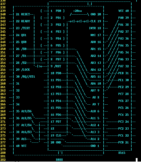
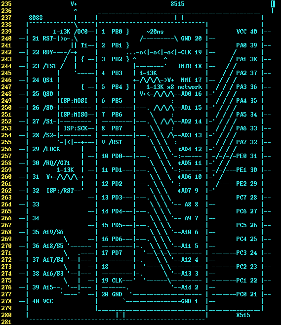
Originally I planned on flipping the 8515 upside-down. GPIO-wise that'd've aligned quite nicely. But most of the AVR peripherals I might use are on PORTB. Also, I want it socketed (maybe I'll replace it with an ATmega162 in the future, etc.). So, instead of flipping it upside-down, I've resorted to rotating it 180deg.
On the motherboard, there's little space at the "top" end of the 8088 (where pins 1 and 40 are located) because of the keyboard connector, otherwise it'd make a *shit-ton* of sense to shift the 8515 "down" (up in the pinout diagram) by three pins.
------
To meet "hold"-times on the bus, the clock-signal needs to be delayed between 10-30ns, because the AVR's outputs occur on the rising-edge of its system-clock. I'll probably use a 74S04 to create the delay. It specs roughly 4ns propagation-delay per inverter. (Wow, I didn't realize how fast the old-school BJT-series could get!) Five of those in series would give me 20ns. And, importantly, also invert the signal.
The 8515 documentation actually says that the internal system-clock isn't perfectly-aligned with the external clock input, and worse that [mis]alignment is device/temperature-dependent.. But, interestingly, it doesn't state that in the section regarding PORT/PIN timings, nor anywhere else I'd seen in 15years of using AVRs. I discovered it recently in the section regarding the External Memory Interface (which most AVRs don't have). (Interesting this information-tidbit never came up during #sdramThing4.5 "Logic Analyzer" or the versions prior, which rely heavily on synchronous operation with the clock-input. Though, this may explain some unexpected timing-differences I'd worked around.)
Thus, using 5 inverters at 4ns would give 20ns delay, which is perfectly inbetween the 10-30ns range. Should I find that doesn't work due to delays in the AVR's external/internal clocking system, I can also choose to tap after 1 or 3 inverters.
Using a 74S04 leaves one inverter for the reset signal... though I'm contemplating whether/how that'll work, since I plan to use In-System-Programming, which needs to drive the AVR's reset signal (and plausibly the entire system's).
--------
I haven't yet verified this, but I'm pretty certain the AVR's clock and reset inputs are compatible with TTL output-levels. Being that many crystal-oscillators have TTL-level outputs, and I'm pretty certain I read that the RESET pin has different thresholds than the GPIOs...
....AND NO. WTF.
AVR:
- Normal pins: VIL<=0.2*VCC, VIH >=0.6*VCC.
- VIL <= 1V
- VIH >= 3V
- RESET: VIL<=0.2*VCC, VIH>=0.9*VCC (!?)
- VIL <= 1V
- VIH >= 4.5V
- XTAL1: VIL<=0.1*VCC, VIH>=0.8*VCC (?!)
- VIL <= 0.5V
- VIH >= 4V
That doesn't even make sense... at 5V, that means XTAL1 has VIL <=0.5V! That's even *lower* than TTL! (Usually CMOS inputs have *higher* VIL-max). And 4.5V for VIH-min?! Heck, the AVR's *outputs* don't even guarantee these values!
OK, got some thinking to do again. Weee!
--------
As for the rest of the circuit... I need to look into the PC/XT schematic, again. My hunch (which, obviously has been wrong before), is that devices don't drive the 8088's data-inputs directly. Otherwise, here's the rationale: Some motherboards have 80C88's and are expected to work with the same ISA cards. *Adding* a buffer (HCT) in between, on these newer motherboards, would add delays which (if the original TTL/NMOS motherboard design *didn't* have a buffer) wouldn't be accounted-for in the timings specified by the original TTL/NMOS design. Thus, the additional delay would have to be accounted for with increasingly complex circuitry and/or wait-states. However, I did read somewhere that an 8088-based system can be upgraded to an 80C88 system by merely replacing the necessary TTL glue with HCT glue... so no extra delays accounted for. (OTOH, aren't HC components slower than LS?).
Now, that's *just* thinking about it from the *timing* perspective. The other perspective is in consideration of output-strength of the devices... There are a *lot* of devices on the bus... a large fanout. 8 ISA cards, the 8088, the DMA controller, timer, keyboard controller, and more. Seems to me, intuitively, they'd've broken that up a bit with buffers (in the original TTL/NMOS design).
Off to find out just how wrong I am...
Oh, so the thought is... assuming there's a 74x245 (TTL) buffer on the data-lines, I could probably swap it out with a 74HCT245, if necessary. Kinda destroys the
"drop-in-replacement" aspect of this project. But, adding a 245 on the AVR's "daughter-board" would be a bit difficult, since the direction-signals aren't driven by the CPU, but from the 8288. Oy.
(And, I still need to look into the other signals, driven by other sources, e.g. the clock-driver handles the clock-output and the READY signal). This is losing its fun-quality fast.
----------
74S04:
- VOH-min@1mA >=2.7V (Nogo. Pull-ups?)
- VOL-max@20mA <= 0.5V (close enough? No way I'm drawing 20mA)
It's somewhat doubtful I have 74HCT's that can be used as inverters in-stock, and that they're as fast as the 74S series... I do have 74ACTs which are even faster, I think... maybe too fast, hmmm... And, not '04s, so I'll probably have to string together a bunch of NANDs.
/RD output!
The 8088, even when running in "Max-mode" (as it does on a PC motherboard) has a /RD output! This guy's unwired on the PC/XT motherboard, so I didn't include it in my pinout. But, if I implemented it in the AVR, it could handle swapping the direction of an "on-daughter-card" 74HCT245... Allowing for a CPU-drop-in-replacement as preferred, rather than having to modify the motherboard. (And, realistically, I could've implemented that even if the original 8088 didn't have a /RD output. Duh). Of course, this'll add a delay... is that a concern?
My current timing-scheme (in a recent log), which has been simplified *dramatically* from earlier expectations, relies somewhat heavily on the fact that only one AVR instruction must be executed during each bus-cycle. BUT, in an earlier (overthinking) log, I mentioned a way to change 9 pins in the same AVR instruction-cycle... The idea is to set up an AVR timer several cycles earlier, with an output pulse when you want it. The /RD pin would be a perfect use for this. (I feel like I read about this somewhere, but I was stupid and didn't bookmark it). At the bus cycle when the /RD pulse is emitted, we also have to change the port to inputs, using up the AVR's one-instruction-cycle during that bus cycle.
Data lines:
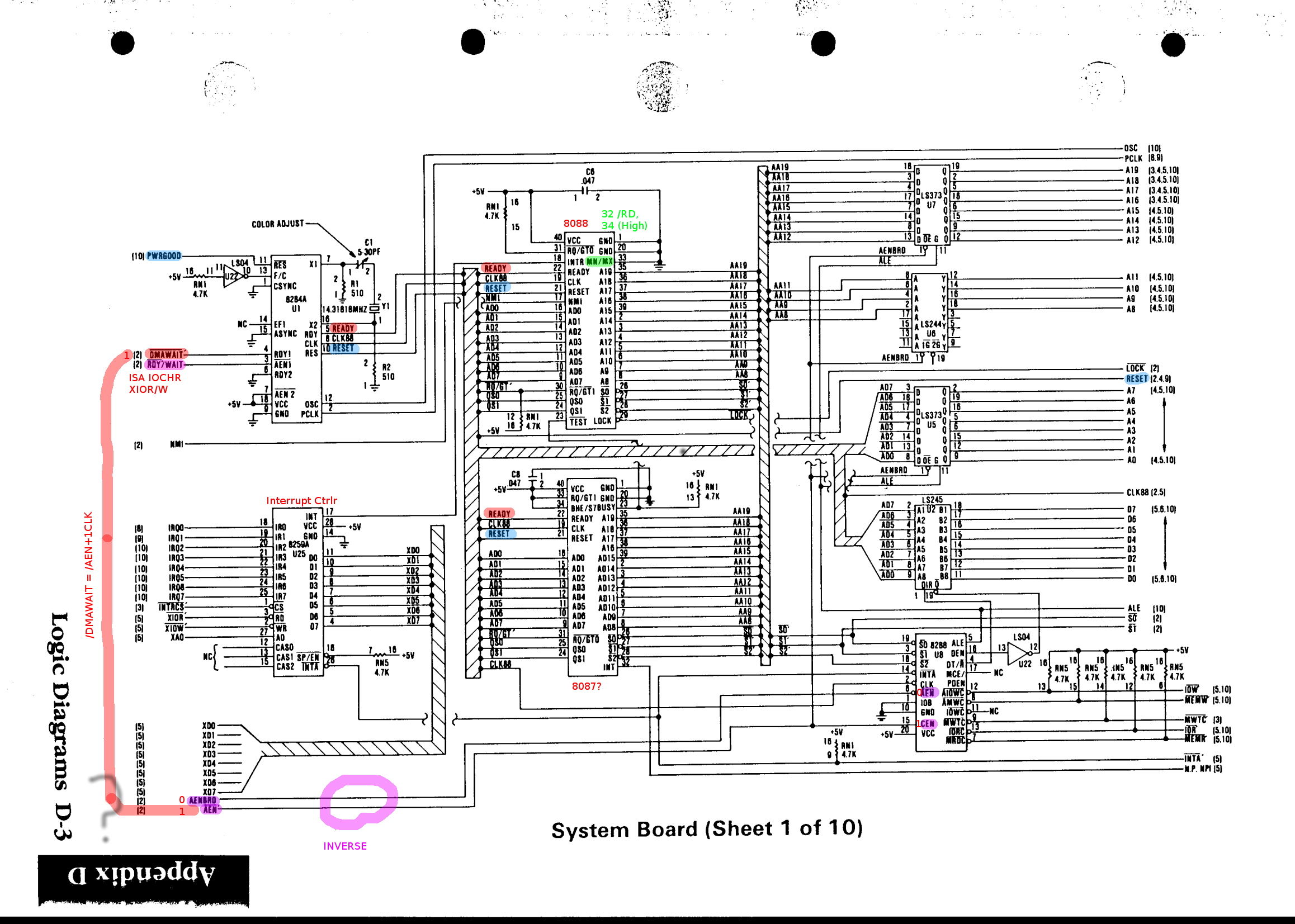
Looking at the schematic, yes, there is a 74LS245 between most devices and the CPU's data lines. The only exception I see is the 8087 which connects directly to the 8088. (I'm not yet implementing 8087 support, and maybe I have an 80C87, anyways?). I think I see this 'LS245 on the motherboard. Unfortunately, not socketed. Or, maybe fortunately since I wanted this AVR-thing to be drop-in...
SN74LS245 (onboard, driving 8088 data-inputs)
- VOL@12mA <= 0.4V (OK)
- VOH@3mA >= 2.4V (Too low. Can I use pull-ups?)
NEC uPD8088D (Same as HMOS-II Intel 8088 Specs):
- VIL <= 0.8V
- VIH >=2.0V (NOT RQ/GT pins! Where are they listed? Nor apparently the clock-inputs?)
- VOL@2mA <= 0.45V
- VOH@0.4mA >=2.4V (TTL-ish)
- VIL-CLOCK <= 0.6V
- VIH-CLOCK >= 3.9V (interesting, similarly different to other I/Os as the AVR's)
NEC uPD8284AD clock generator (CLK / READY -> 8088):
(CLOCK output, doesn't really matter since I've got to drive it through an inverter, anyhow. But READY is a concern).
- VOL<=0.45V
- VOH-CLOCK@1mA >=4.0V
- VOH-other@1mA >= 2.4V (e.g. READY, too low... pull-ups?)
-----------------
AVR inputs are rated for -0.5V to VCC+0.5V... could this be useful?
I'm not building a product, here... I just want to get programming!
So, let's say we ran the AVR off 4.5V, instead...
- Normal pins: VIL<=0.2*VCC, VIH >=0.6*VCC.
- VIL <= 0.9V (was 1V)
- VIH >= 2.7V (was 3V)
- RESET: VIL<=0.2*VCC, VIH>=0.9*VCC (!?)
- VIL <= 0.9V (was 1V)
- VIH >= 4.05V (was 4.5V)
- XTAL1: VIL<=0.1*VCC, VIH>=0.8*VCC (?!)
- VIL <= 0.45V (was 0.5V)
- VIH >= 3.6V (was 4V)
Specifications listed earlier for other chips are mins/maxs... NOT typicals. And, in many cases, ratings given for much greater loads than the AVR (and other circuitry) would impart.
Kinda ironic, The 74S04 happens to have VOH >= 2.7, which now meets our VIH... except it's not connected to a GPIO, but to the XTAL1 and RESET inputs, which it's not even close to meeting specs for. And the 74LS245 --which does drive the pins that are now capable of VIH >= 2.7V--(as well as the clock-generator which drives READY) only guarantees VOH >=2.4V.
Weee!
---------------
I guess, then, there's good reason I've been lagging on actually soldering this stupid thing up... Looks like I'll be needing more support-circuitry than I planned to make this even reliable enough to experiment with. weeee...
--------------
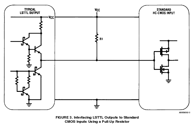
Pull-up resistors for TTL -> CMOS:
I knew I read it somewhere...
https://www.fairchildsemi.com/application-notes/AN/AN-314.pdf
Since LSTTL specifications guarantee a 2.7V output high level instead of a 3.5V output high, when designing to the worst case characteristics greater compatibility is sometimes desired. One solution to increase compatibility is to raise the output high level on the TTL output by placing a pull-up resistor from the TTL output to VCC, as shown in Figure 3.
When the output pulls up, the resistor pulls the voltage very close to VCC. The value of the resistor should be chosen based on the LSTTL and CMOS fanout of the LS gate. Figure 2 shows the range of pull-up resistors values versus LS fanout that can be used. For example, if an LSTTL device is driving only CMOS circuits, the resistor value is chosen from the left axis which corresponds to a zero LSTTL fanout

I'm not too fond of adding more chips to this thing, so I'll use some rationalizing to justify why people might choose HCT over pull-ups *besides* the likely speed-increase (since 4.77MHz isn't *that* fast, right?).
My rationale for the use of HCTs over pull-resistors is that they can easily be dropped-in-place of other chips that already exist (like the 74LS245). But, since my '245 is soldered-in, and I don't want to modify the motherboard to make this work, that'd mean I'd have to add *another* HCT245 inbetween. So, whatever speed-increase may be gained by using a HCT245 *as* your receiving CMOS device (rather than adding pull-ups) won't be gained, here, because the HCT245 would be inserted *between* the sender and the receiver. So, it'd probably be faster, anyhow, in this case, to just use pull-up resistors. Whew. Network-resistors are easy.
No mention of how to *calculate* the VOH value you'll get when using a specific resistor-value... but my theory is that since the LS high-side driver is, essentially, an emitter-coupled voltage-follower, the pull-up resistor will, essentially, cause the high-side NPN to turn off (the pull-resistor's voltage would be higher than the base). That's my theory, and I'm sticking to it.
So, now... That leaves us with... If this is driving anything *other* than CMOS, there might be trouble, because the pull-resistor might act as a voltage-divider with whatever else is connected.
So, now... I need to make sure wherever I'm throwing these pull-resistors won't be connected to anything other than CMOS inputs.
---------
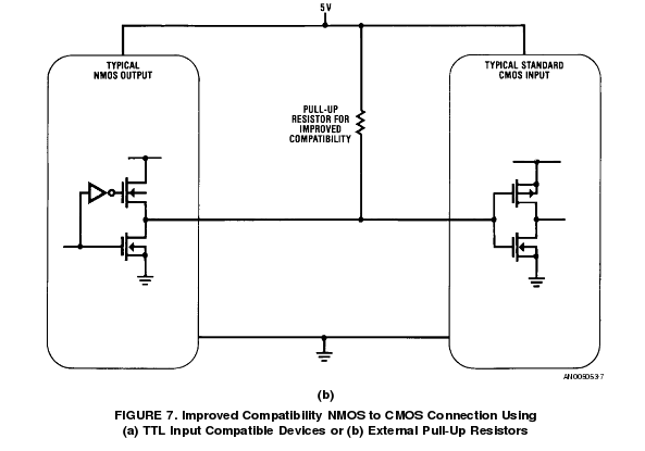
From there... There's another consideration. Some of our sources *aren't* TTL, despite having TTL-level outputs. The clock-driver appears to be NMOS or HMOS.Thankfully, that same document has a discussion about H/NMOS as well, and says that it can be treated similarly to TTL. Add Pull-Ups.
Which, realistically, is probably the same for TTL when very weakly-loaded (as will be the case in this circuit), and I could've probably just wired the danged thing up as I'd originally planned without messing with any of this.
--------
So, back to the schematic... Do I need to worry about voltage-dividers when using pull-ups?
The only CPU inputs being implemented, thus far, are AD7:0 (data inputs), CLOCK, and READY. CLOCK is connected to my 74S04, or whatever... So pull-ups are occurring *after* the 74S04. The only load is the AVR's CMOS inputs. OK. READY looks like it's only connected to the 8088 and 8087... 8087's Not Yet Installed (and is HMOS, anyways, which allegedly looks like CMOS, load-wise). So, no problem there. Now, DATA.
DATA, when reading (when we'll need to use the pull-ups) comes from the LS245, and fans-out to the 8088 and 8087, which should be fine. But ALSO routes to a 74LS343.
The '373 input *might* interact with that pull-up resistor to create a voltage-divider, in which case it kinda nullifies its purpose. Funny they didn't mention that in the .... wait... they did! Figure 2.OK, LSTTL-Fan-Out = 1. and CMOS-Fan-Out doesn't count. So, allegedly, I can get away with a pull-up resistor anywhere from 1-13Kohms. I'm pretty sure I've got some network-resistors in that range.
Nice. And this thing should work...
The only problems, then, should be my lack of understanding of the bus... software... right?
Now I want to get this blasted thing running. But beer sounds a lot better, even if it is alone on a Saturday Morning and will leave me literally flat-broke until... Wednesday(!?)
-------
But first... What was my beef with the 74S04 that might lead me down a different route...? Didn't I mention ACT NANDs or something...? Nothing, nothing we haven't already covered... Pull-Ups will fix it.
So, we should be at the point where I can solder this danged thing up and ...
Nope.
RESET and the In-System-Programmer.
The RESET input is one-way... The clock-generator chip is responsible for the RESET signal, and it's apparently not open-collector. So, the ISP's /RESET signal won't reset the rest of the system, and must be isolated from it.
OY.
On the plus-side, I've left PORTB un-mapped, so far... And that's where the ISP pins connect. So, for these early experiments, I don't have to worry about what the rest of the system is doing while the ISP is programming. WHEW. (Note to self, remove hard disk for these experiments!)
(NOTE 1-31-17: I've just checked, and the 8284 clock/reset/ready generator chip does *not* stop outputting the clock signal during reset. Otherwise there might've been some difficulty ISProgramming an AVR whose clock is externally-driven. OTOH, the ISP's reset signal will *not* feed back into the motherboard, so I guess it wouldn't matter anyhow. AND the reset signal apparently *only* happens during power-up, as it's only tied to the Power-Good signal. Interesting.)
So, I'll take the output from the 74S04 and feed it through a diode, thus making it essentially open-collector, active-low-only. OK.
This should do...
Discussions
Become a Hackaday.io Member
Create an account to leave a comment. Already have an account? Log In.
That is some fine ASCII artwork!
Are you sure? yes | no
Thankya, Sir!
Dunno why, but I haven't been able to get myself to draw schematics with schematic software for well over a decade... and when I make PCBs I enter netlists by-hand. Weird world I live in. At least I've moved back up to electronic rather'n paper schematics, and on the plus-side, least I haven't been using Eagle for schematic-entry for all these years!
Are you sure? yes | no
@Stuart Longland, not a bad idea. I actually have a couple graphics-tablet options. Never thought of using 'em for schematics.
Actually... I do most of my schematics on paper, first... then when/*if* I'm in documentation-mode I do the ASCII art to verify my pinouts and functionality... That mode usually happens right before coding, to map pins with #defines, and keep everything together.
Computers are nice, but not nearly as portable and robust as paper... most my schematics have solder-burns ;)
Are you sure? yes | no
[this comment has been deleted]
Indeed, re: the edit. I could imagine it'd be easy to miss something in that schematic... was tough to fit in 80 columns.
Thanks for the heads-up on the diode. Despite all my ramblings about voltage-levels, I completely forgot to consider the voltage-drop across the diode, which may be a problem. And switching-speeds as well. I probably have some high-speed Schottky I could scrap from scrap PCBs... but that wasn't in my original plans. Wee!
Maybe an NPN is the way to go... make it a real open-collector output. Or maybe use a 74S05, instead of the '04. I dunno why, but using discrete mosfets almost never crosses my mind.
Looks like whatever I do, I should probably leave some spare protoboard space ;)
Are you sure? yes | no
@Stuart Longland, nah, schottky should be fine, 1V VIL-max... But I was planning on throwing in a 1N914... ;)
'05 might not be a bad way to go, but it also requires 4 additional resistors... at which point an NPN takes less space.
I'm on the opposite end of the spectrum, it's afternoonish, but I've been at it since last night. Caffeine might've caught the diode problem. But I don't think it'd get me soldering any sooner.
Are you sure? yes | no