 Eric Hertz
UPDATE 2-3-16: Adding fan-out info from the schematic (which isn't to be trusted)
UPDATE 2: and measurements from multimeter, + experiment with pulling down /LOCK.
-----------
Thoughts on possible 8088 outputs which are currently unimplemented that might help if they were...
Currently unwired (floating) 8088 outputs:
/LOCK - Pulling this low would likely assure that no other devices try to access the bus... (They shouldn't, since they haven't been initialized to do-so, but this shouldn't hurt). When active, devices shouldn't request to use the bus. Doing this would be a bit of a hack-usage of the signal but should be within-specs of the devices connected. Also, I don't see it's being pulled by resistors in the schematic, so currently it's floating. WHOOPS. Regardless, whatever it floats to, it shouldn't be paid-attention-to at this point, since, again, nothing that uses it has been initialized. But, floating-inputs have strange effects, sometimes...
[/LOCK Schematic Fanout = 1 LSTTL load, no pull-resistors. Pull-Down of LSTTL needs something like 330ohms!]
{Measuring diode-drop to V+... Yep... Floating input? Tied to ground with 100-ohm resistor, no change.}
/RQ / /GT1 - Pulling this high should do the same as /LOCK... (Note that both RQ/GT signals are pulled-high in the schematic, and /RQ / /GT0 is otherwise unwired). Any device requesting to use the bus would be denied. NOTE that since this is a bidirectional signal, and since the active-level is the same in each direction, the pull-up resistor needs to be small-enough to overcome *any* capacitance on the line *before* the next clock-cycle. Hmmm... (Would think that'd be inherent to the system design, but should probably look into this. Probably wouldn't hurt to pull it higher).
[/RQ / /GTn Schematic Fanout: RQ/GT0 = 0, pulled up via 4.7K; RQ/GT1 = 1 HMOS (8087), pulled up via 4.7K... Pull-Up, if not already, 10K should be OK]
{BOTH measure 4.7K to V+}
QS1:0 - Pulling these low should prevent any devices which use them (isn't that only the 8087, which isn't wired?) from ever trying to take over the bus... by tricking those devices into thinking every read-operation from the "8088" (AVR) is actually a memory or I/O read rather than an instruction-read which they might need to process. These guys aren't pulled-up in the schematic, but also looks like they're only wired to the 8087, which isn't installed.
[QS1:0 Schematic Fanout = 1 HMOS (8087), no pull-resistors. Fanout to HMOS, 10K pull-down should be OK, if there's a stray LSTTL not in the schematic we'd need more like 330ohms!]
{Not measuring anything between here and V+/GND. (8087 not installed). Maybe otherwise N/C.}
OTHERS:
Pin 34 - This pin is allegedly "always high" (output)... It shouldn't be wired anywhere, and is not shown on the schematic. But this motherboard is a clone, so who knows.
[Pin34 Schematic Fanout = 0, Allegedly N/C]
{Not measuring anything between here and V+/GND. Maybe N/C.}
/RD - The 8088, even in "maximum mode" (where it uses the 8288 to generate the /RD and /WR signals, as is the case in a PC/XT) outputs the /RD signal to one of its pins (why?!). The schematic shows it as N/C (logically). But, again, this is a clone, so I'd better verify that.
[/RD Schematic Fanout = 0, Allegedly N/C. If this is used on this mobo, then what???]
{Not measuring anything between here and V+/GND. Maybe N/C.}
/S2:0 = 0b100 - This indicates "Code Access" TODO: What makes that different from a Read-Memory (0b101)? Do the 8288's outputs respond differently, or does this go along with /QS1:0 to deviceswhich use them...(like the 8087)? Presumed: Code-Access only works on the memory-bus, anyhow (as opposed to I/O), and only as Read, and memory-devices (ROM/RAM) shouldn't care whether it's code or data, as far as how they respond...
Schematic-wise: /S2 is only wired to the 8088, 8087, and 8288... so shouldn't matter, for now.
/S1:0 is the same, but is also wired to a 4-input AND gate. 00, 01, 10 should have the same effect, regardless; forcing the output of the AND gate low, regardless of the other inputs. (Which seems strange, because its other inputs include the DMA-request, which would only be allowed when 11, which could occur during *both* "passive" (idle) mode, or "halt." Huh.) This same AND gate is also driven by /LOCK, so as long as that's low, that should do the same, here, as assuring that /S1:0 is never 0b11.[/S2:0 Schematic Fanout = 2 HMOS (8087, 8288) + 1 LSTTL (/S1:0). Not particularly relevant, since these are driven by the AVR.]
Also interestingly, the DMA request/grant scheme looks to rely only on whether the 8088/8087's bus units are idle (or halted), rather than the DMA controller's actually requesting a hold from the 8088. Which, looks like it's glue-logic implemented to have a 2-cycle delay guaranteed response of acknowledge, regardless of what's happening at that time (e.g. the bus was idle two cycles ago, but what if it's not NOW?). Not wrapping my head around how that'd *ever* work, considering the only time the bus would be idle (unless explicitly requested) is when the BIU's instruction-queue is full and no memory accesses are occurring (which seems quite seldom, considering the KIPS math I did earlier suggesting that the 8088's limited number of KIPS has more to do with the bus-bottleneck than its actual instruction-execution speed). Weird.
Here's a snippet:
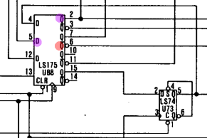
The clear input to the LS74 is driven by HRQ_DMA, from the DMA controller, the Q output goes to HOLDA (at the DMA controller). As I recall, Clear and Set on a '74 affect the outputs regardless of the clock-input. If HRQ_DMA is high, and /LOCK and /S1:0 are also high, then pin13 on the LS175 is high. Oh, The LS74's Clear input is active-LOW, so cleared when the DMA controller is *not* requesting a hold. When *not* requesting a hold, the /Q output is high, which causes the Q output to be low, and thus HOLDA is inactive. OK.
When a hold-request is placed, regardless of the 8088's usage of the bus, the clear
input goes high, but Q (and thus HOLDA) is still low, from before, and /Q is high. OK.
Assuming the HRQ_DMA pin *stays* high AND the processor doesn't start a
new transaction* (and/or finishes one)... (for at least one more clock cycle) the D-input will
become high, the Q output (and thus, HOLDA) will follow on the next
clock-edge (which is actually inverted on the LS74). The /Q output will
then go low on that same clock-edge, which causes a "Set", the Q output
will be forced to remain high, regardless of what happens on the D
input. OK. (Wait, what? What if the CPU starts a new access?)
The HOLDA output (Q) feeds into the DMA controller, acknowledging the hold-request. Maybe then, or maybe later (after the DMA transaction?) the HRQ_DMA pin goes low, which pulls the LS74's CLEAR input active. Here's where it gets iffy. The LS74 has a strange state: When BOTH Set AND Clear are active (which they would be, here), BOTH outputs go high. OK. Q was already high. A high on /Q causes Set to be deactivated, but Clear is still active, causing Q to go low. OK. And as long as HRQ_DMA remains low (inactive) the HOLDA pin ignores D, remaining low... OK.
*Now, what happens if the processor starts a new transaction after HOLDA...? (And it looks like it could, for at least a couple clock-pulses thereafter!) The D input goes low. And we're assuming HRQ_DMA remains high, so the LS74's Clear input is inactive. Then D->Q. But No. Because Q was high, which means /Q was low, which means SET is active, which means the D input is ignored, which means the 8088's transaction will be ignored, which means the DMA transaction will still continue. SO, HOLDA (OR HRQ_DMA, as I would've assumed) must somehow be fed back to the CPU to prevent it from starting a new transaction.
But the only path back to the CPU appears to be via the READY/WAIT input... which doesn't *prevent* a transaction from starting, but causes an already-started transaction to wait for a while before completing. WHICH MEANS the 8088 will drive the address-bits at the same time as the DMA controller.
EXCEPT. There's another path from HOLDA that feeds into the 8288 controller. This disables commands and disables the address-latching... AND, all the 8088's address-bits are latched onto the address-bus via the 8288. OK.
INTERESTING.
So, if I understand this correctly... the 8088's READY input, in this case, tells the processor's bus-transaction, which has *already started* to WAIT.
But wait-states are only inserted AFTER T3.
And T3 is AFTER the processor has performed *several* transaction-functions... Including writing the address-bits, and latching them, and turning the address/data port into inputs for reading-back data, or writing the data bits to the port... It looks like the ALE output of the 8288 still functions, causing the CPU's address-latches to latch properly, but the output-enables aren't yet driven (by the same feedback path, from the HOLDA signal that stalls the 8288). OK... so the 8088 has *started* a transaction, (in fact, the majority of the transaction has already occurred) but the transaction is held via (indefinite) wait-states. The 8288 still *sees* the transaction, and follows-along in whatever internal state-machine it may have, but many of its outputs are disabled. So, it still follows-along with the 8088's transaction until it stalls.
(Bummer, I thought for a second, there, this arrangement might've been confirmation that the 8088 could interact with the 8288 more similarly to how I'm attempting with the AVR... e.g. setting up the address signals *way* before starting a transaction, etc.)
OK then. Interesting result 2: The READY signal *can* be stalled indefinitely (at least as long as the longest DMA burst!). That definitely seems to be confirmation that inserting "artificial" wait-states from the AVR's slow processing-time, should function. WHEW!
No... EXCEPT that, the 8288's Command Enable input is indirectly driven by the same source that deactivates the READY signal... so... IF it is a state-machine driven by clock-edges *until* T3, whereafter it masks the clock-signals by the CEN signal, there's no path for the processor to insert wait-states. IF it's NOT that sort of state-machine, but one wherein it acts on clock-edges *until* T3, whereafter its clock-signals are masked by the processor's /S2:0 outputs' not going "IDLE", then it should handle wait-states inserted by the CPU. (this is the case I presumed). HMMM...
I haven't seen anything to that level of detail in the datasheet.
That said, It also looks like the only two sources of READY's being deactivated are from IOCHRDY (from the ISA bus, which I'm not using) and the DMA controller (which I'm not using), SO, I should be able to get away, in this early stage, *without* the processor's reading the READY signal, at all, when accessing normal memory-locations (RAM or ROM) and just "dead-reconning" the number of bus-cycles. In which case, the system should've worked already, as-implemented, with a couple NOPs here and there, as long as my timings are correct.
Interesting result 3: The DMA controller can't be interrupted by the processor?!
Interesting... that might explain why e.g. the entire computer seems to stall when accessing floppy drives, etc. Surely they improved this in later systems, e.g. those that can run WinXP... Or do they just rely on the idea that most everything that needs to run (at least the mouse interrupts, etc.) is cached...? Weird.
See the problem...? I don't... That circuit's way too friggin' loopy.
Discussions
Become a Hackaday.io Member
Create an account to leave a comment. Already have an account? Log In.