 Eric Hertz
UPDATE 3: DRAM CAS/RAS via delay-line... interesting. At the bottom.
UPDATE 2: Yep... DRAM latches on falling-edge. At the bottom.
UPDATE: Surprising result added at the bottom
-----------------
Seemed like a simple step from read to write... but so far it appears to be writing the low address byte to the DRAM, rather than the data.
This is kinda confusing... Or at least, surprising.
I'm not familiar with DRAM (SDRAM, SRAM, a bit... but not DRAM).
So maybe there's something in there...
If this were SRAM: As I recall: When the /WE pin is active, it'll write to the selected address. So, if the address stays constant (which it does, since it's latched), the data could change numerous times before the /WE pin is deactivated, and whatever was on the data-port last (assuming a long enough setup/hold time) would be stored in the memory.
So, e.g., it would be doable to wire the SRAM's data pins to the shared/multiplexed Data/Address port, to load the address to that port, to latch the address (in an external latch), then enable /WE (with the address on the shared address/data port!), then (after /WE) change the low address/data port to the data to be written (address has been latched, remember?)... let it "stabilize" there for a bit, then disable the /WE pin. Technically, the memory-location would store the low-address-byte for a brief time, but then it'd be overwritten with the data... so, as far as anyone would see, it'd look like it worked as-expected, were the /WE pin *only* active when the data was on the port.
This is, entirely, as I recall... I could be mistaken. Regardless, certainly whatever's loaded is that which was valid when the /WE pin toggled from active to inactive. Right?
----------
Frankly, it shouldn't matter whether DRAM works differently, as long as it latches the data when /WE deactivates. And, frankly, it shouldn't be any other way... because... the bus could be held-up by wait-states (which apparently has less to do with the actual time it takes to access slow memories than it has to do with waiting for other things holding up the bus, e.g. DMA... per my understanding of the schematic).
Which Means...
...No. Because if the bus is held-up, the READY signal indirectly deactivates the 8288's CEN input, which disables the /WRITE signal. (and, oddly, causes the timing-diagram to be distorted, because /WRITE is shown active during T3, but with CEN disabled (which is supposed to happen before T2), it would become active *after* CEN is reenabled.
OK... So, it's plausible... Though completely beyond my intuition, that data is stored upon /WE's activation. edge-triggered on the opposite edge I'd've expected...(?!)
Let's pretend that's the case for a second...
Then timing needs to be much more precise than for read-operations.
And uC-inserted "artificial wait-states" won't work... at least with regard to being able to use that time to help set up data. (They do, however, still appear to affect the deactivation of the 8288's /WRITE pin, as 'scoped).
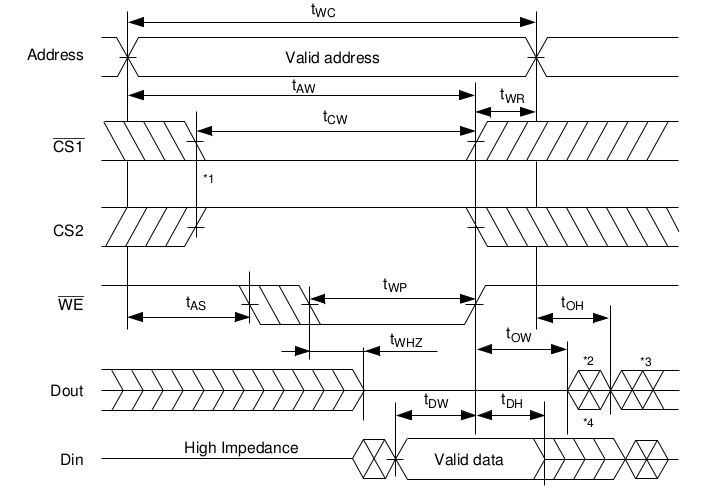
That timing-precision...? Because the address has to be latched, which happens near the end of T1 (and requires a hold-time thereafter), then the data has to be available by the beginning of T3... Only slightly longer than one clock-cycle. Which should be *plenty* of space to work within, but also quite a bit more timing-sensitive than the read-operation... So maybe those inverter-clock-delays and cycle-counting with NOPs are more important than read-back led me to believe.
This, too, might suggest that even if I get one device working smoothly with whatever wonky timing-scheme I might come up with, doesn't necessarily mean it'll work with another... So maybe it's a good thing I spent so much effort looking into those timings early-on.
Got some 'sperimentin' to do. First things first: Clock-Delay jumpering. Then NOPs that can likely be removed (carefully! Keeping clock-delays and setup/hold times in mind!). And, from there...? I read somewhere the AVR's internal clock doesn't necessarily align with the external clock input... so might be necessary to characterize that, a bit.
Kinda funny, I thought write would be less timing-sensitive than read...
-------------
Another possibility supporting the awkwardness of /WE's apparently latching on its falling-edge could be an intermediate data-latch that I'm not seeing. I glimpsed through the schematic and don't see it, but who knows. The DRAM circuitry's a bit complex, what with row/column strobing, etc. (Before I started this project, it hadn't occurred to me they would implement that scheme with simple logic gates, making it *look* like a regularly/linearly-addressed memory. Interesting ponderance to throw at #sdramThingZero - 133MS/s 32-bit Logic Analyzer)
Interesting observation:
The DRAM (even this really old stuff) apparently retains its value for *quite some time*. I turned off the computer for several seconds and it still read back most of the data written.
------------------
UPDATE: Huh, removing this NOP gives darn-near 100% write/read verification...
I'm pretty certain that nop needs to be there. And changing the AVR's clock-delay doesn't seem to have an effect. Definitely some thinking to do.

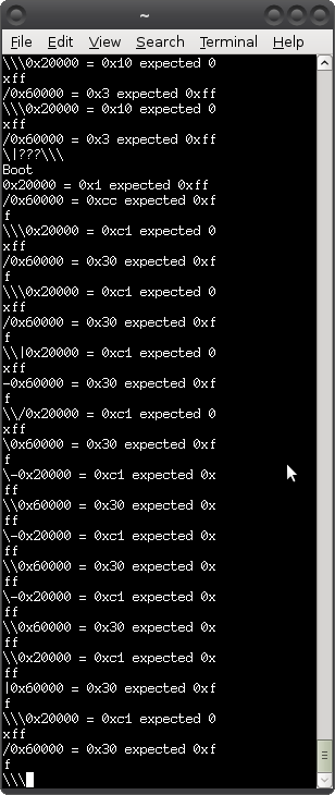
brainjuice running out... interesting pattern, though.
--------
SRAM:
Latches on rising-edge...
DRAM:
Latches on falling-edge.
------------
Am thinkink the reason the 8088 bus-timings are *so strict* is because it's meant to work with various different devices. So, for instance, can probably handle both SRAM and DRAM. (And here I thought these interfaces were pretty much standard... why call it /WE at all? Why not WE, or better-yet WCLK... wait, isn't there a "C" in the 8288's write-signals... hmmm... /MWTC "Memory-Write COMMAND" heh.)
--------------
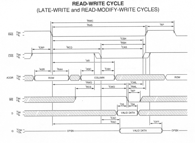
Check this guy out:

So basically the Row-Address is strobed, then a delay-line(?) signals to load the column-address, then creates the Column-Address strobe.
And I've yet to find anywhere where an onboard memory-device requests wait-states... (only the ISA cards and DMA, so far). Interesting that all these subsystems are running at, basically, the same speed. DRAM I'd've thought would be slower, at the time. Not only slower, but also slowed by the fact of random RAS/CAS accesses. And, yet, if I understand this correctly, the DRAM actually responds to a full-speed 8088 bus transaction with no wait-states. Similarly, the ROM/BIOS... Would've expected EPROM accesses to be somewhat slower than RAM... And all the logic propagation-delays (and a delay-line!) everywhere...
Discussions
Become a Hackaday.io Member
Create an account to leave a comment. Already have an account? Log In.
Are you sure? yes | no