With a better understanding of the physical layout, we can start to figure out how to load bits into this thing to get some blinkenlights happening.
The module is divided into three identical banks, and each bank has separate, identical connections, so we will just focus on a single bank and know we'll have to do everything X3 for get the whole panel working...
The TLC5941 is a 16-channel, 12-bit-per-channel, PWM capable LED driver with dot correction. They can be chained together by linking the serial out (SOUT) of one chip to the serial in (SIN) of the next chip in the chain, and driving the serial clock (SCLK) of all chips in the chain with the same source.
Each of the 16 channels takes 12 bits of data, so fully loading one driver requires clocking in 192 bits. This 12-bit value is used by the PWM control to specify its brightness (0x000 = 0%, 0xFFF = 100%).
Each bank is three groups of three chained-together drivers. Each of these groups is a color channel: Red, Green, and Blue. All three groups share the common control signals but have separate SIN lines. Since there are three chips chained together per group, you will need to clock in 576 bits per color channel to fully define that bank's colors.
Data is shifted into (and out of, via SOUT) the input register. When all of the data is loaded, a signal is given to transfer the input register to the output register, and the output is updated. This lets you clock in new data while the previous data is still being displayed, which reduces glitchyness. Data is clocked in one bit at a time, most significant bit (MSB) first.
The common control lines are:
BLANK: When BLANK is logic high, all outputs are disabled (but the data in the output registers is retained) and the PWM counter is reset. BLANK is pulled high just before the XLAT line is used to transfer data from the input register to the output registers. Resetting the PWM counter is also critical to the operation, and I'll describe that more under GSCLK. Pulling BLANK low will re-enable the output causing whatever data is in the output register to be displayed.
XLAT: Transfer latch. Pulling XLAT high (ideally, while BLANK is also high) will transfer the contents of the input register to the output register. It will also fill the input register with status data, which you can then clock out into your controller, however these modules do not have any connection from the SOUT of the last chip in each chain so getting that signal will require some mod wires.
SCLK: Serial clock. Each pulse of SCLK will shift the input register left by 1 bit, putting the MSB into SOUT and filling the LSB with the state of SIN.
MODE: Programming mode. When MODE is low, SIN and SOUT are connected to the 192-bit input register. When MODE is high, SIN and SOUT are instead connected to a different, 96-bit register (6 bits per channel) that controls the dot correction. Dot correction allows you to set a constant offset for each channel to correct differences in brightness from one LED to the next.
GSCLK: Greyscale clock, aka PWM clock. While the driver has an internal PWM counter, it relies on an externally supplied clock to increment this counter. When BLANK goes high, the PWM counter register is reset. When BLANK goes low, the PWM counter will be incremented by 1 on each rising edge of GSCLK. When the PWM counter matches the input value for each individual channel, that channel output is disabled. The PWM counter must be manually reset by toggling BLANK high then low. Failure to cycle the BLANK signal means the output will get disabled as soon as the PWM counter is up and it wills stay off. In practice, since each channel is 12-bits, you should cycle the BLANK line every 4096 pulses of GSCLK.
Okay, so now that we know what the data lines do, let's discuss how to actually load data and get this thing working...
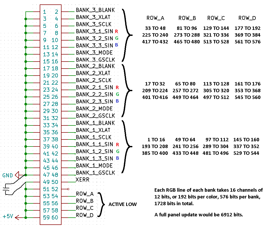
Let's say we want to light up LED1 (top left corner) solid RED at 100% brightness. LED 1 is bank 1, row 1A, and we're just worried about the Red channel right now.
First, remember that all of the data is most significant bit first. We will need to load 3 rows worth of data - 576 bits - but the most significant bit is going to be the end of row 3. For bank 1, that will be LED400. LED1's data will be the last 12 bits clocked in.
So we clock in 564 zeroes, and 12 ones, filling channel 0 of chip 1 with 0xFFF.
Now we set BLANK high to temporarily disable the outputs so we can set those outputs without any craziness, and then pulse XLAT to copy the input bits to the output bits. Setting BLANK low again enables the outputs and... nothing!
Well the most obvious thing is obvious: We need to enable the MOSFET for that subrow. We do this by pulling ROW_A (per the above diagram) low. Huzzah! Still nothing!
We will get no output without the GSCLK to drive the PWM controller! So now we start pulsing GSCLCK as slow as we please, or up to 30MHz. One the PWM clock has completed one full cycle, the light comes on! Then immediately goes off again?
The reason it only blinks is because we're not resetting the PWM counter. Once the PWM counter reaches the value of any channel's 12-bit value, that channel is disabled until the PWM counter is reset. We reset it using the BLANK line. So now we have to count 4096 pulses of the GSCLK, pulse the BLANK line, and repeat.
This is a pain in the butt, however it's not like we can't do anything useful during that time; Recall that we need 576 bits to load all of the data into the drivers, so even if SCLK is a quarter the speed of GSCLK, we have enough time to load entirely new values and refresh the display! Don't forget to use XLAT to move the data between registers while BLANK is high!
Ah but there's good reason to want the SCLK the same speed, or faster, than GSCLK: To drive the entire bank - all 16x12 LEDs - we need to load the data for the next sub-row, then switch the MOSFET drives to that sub-row, then set BLANK to low. Now our drive logic looks like this:
1 - Clock 576 bits into each of the R, G, and B lines
2 - Set BLANK high
3 - Pulse XLAT to set the data into the outputs
4 - Enable the subrow MOSFET
5 - Set BLANK low to turn LEDs on
6 - Pulse GSCLCK 4096 times
7a - While doing step 6, start with step 1 for the next subrow but do not proceed to step 2 yet.
7b - Once you reach 4096 pulses of GSCLK, continue from step 2
Assuming SCLK and GSCLK are running at the same frequency, you have more than enough time to do all this and even a little bit of time left over for other processing... you'll send 2304 bits of data (thus 2304 SCLK pulses) and 4096 GSCLK pulses per full refresh.
Now multiply all that for banks 2 and 3, and you're driving the whole panel! One caveat though: The MOSFETs control the entire panel, not per-bank, so each bank needs to be updated in synch. Just keep that in mind.
Discussions
Become a Hackaday.io Member
Create an account to leave a comment. Already have an account? Log In.