0%
0%
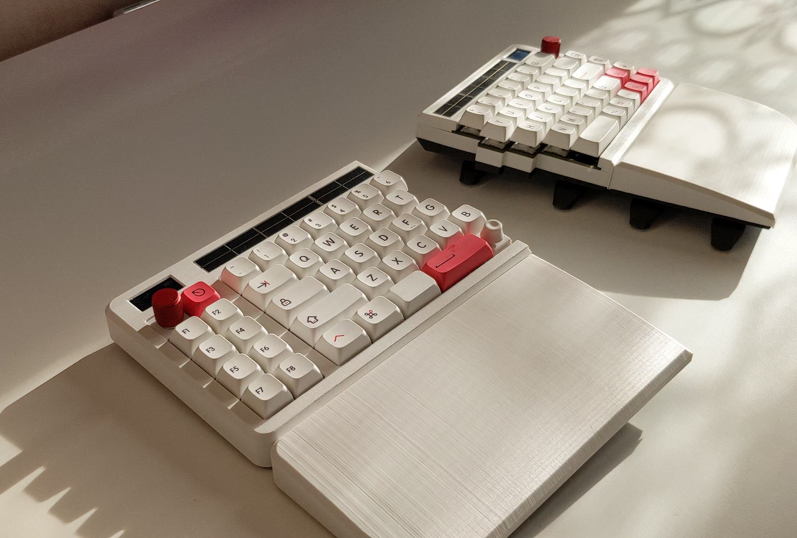
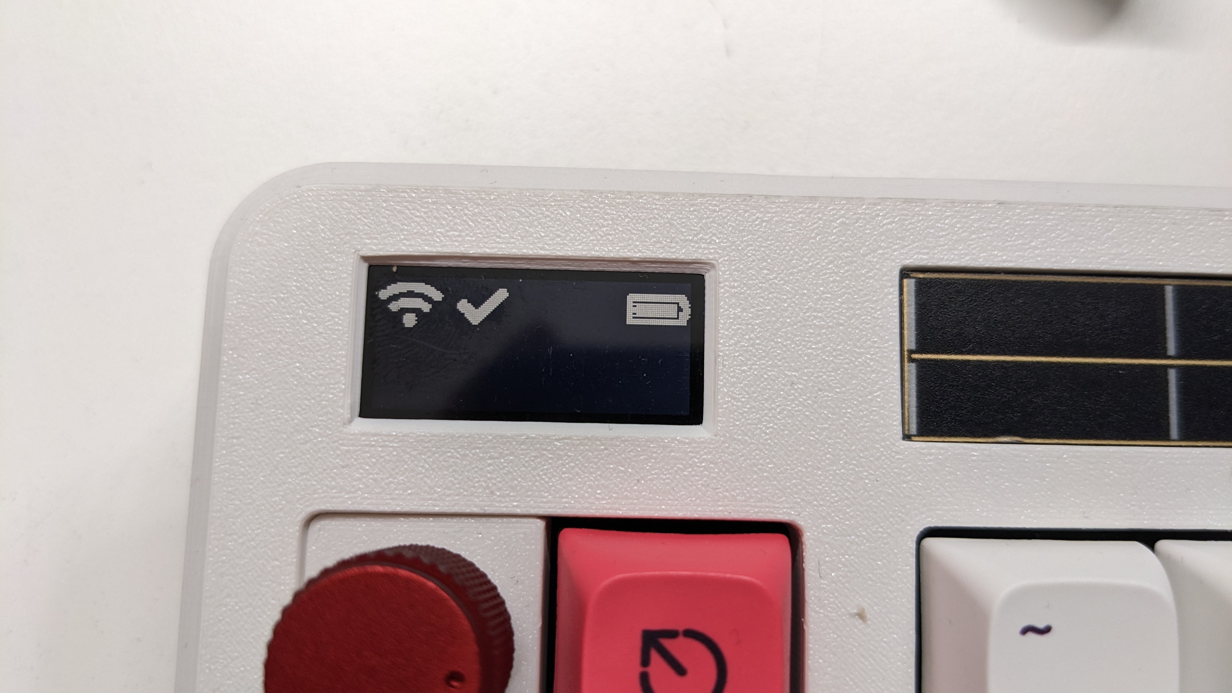
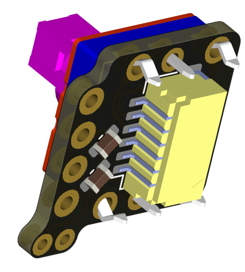
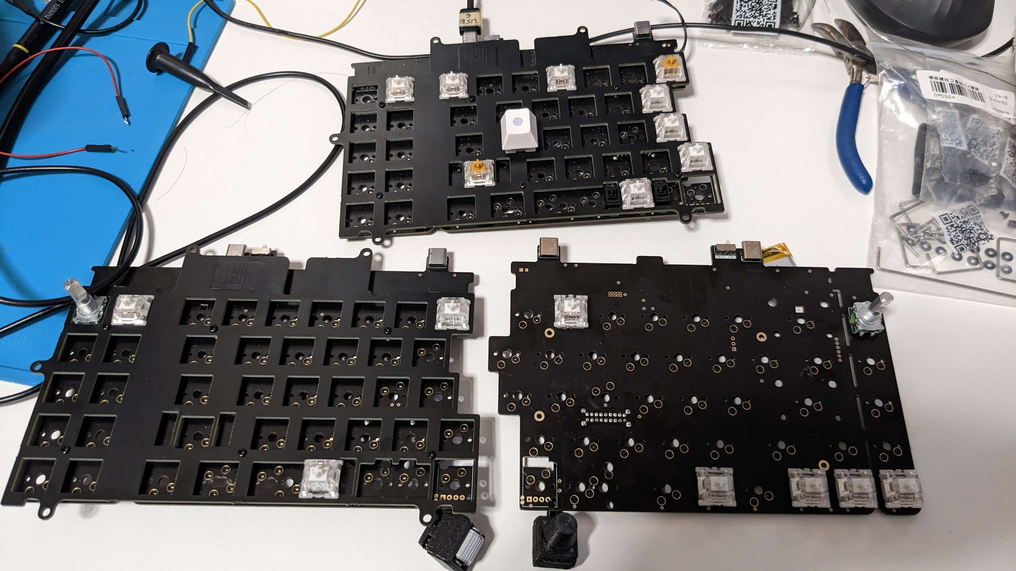
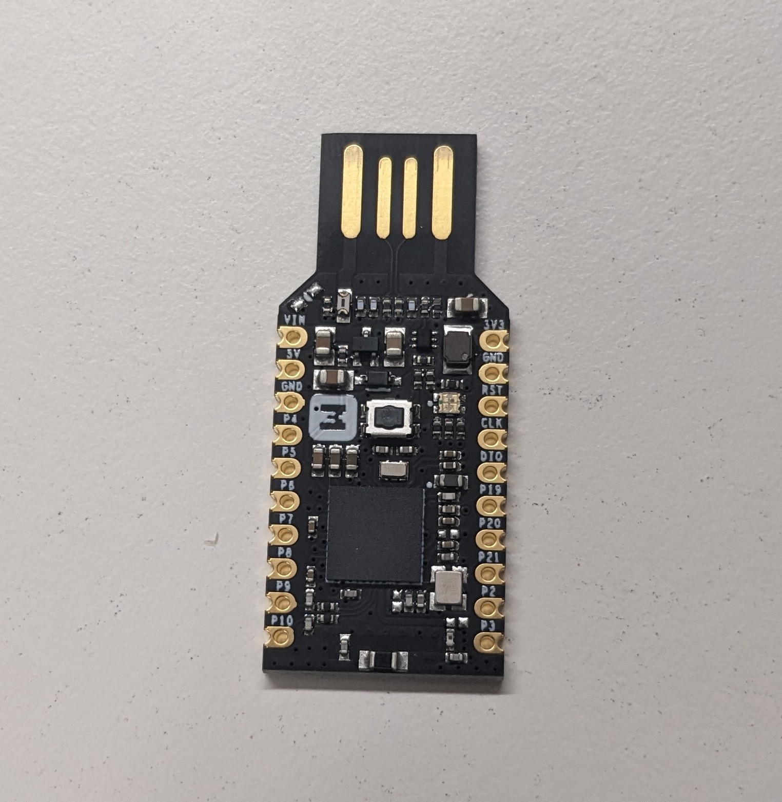
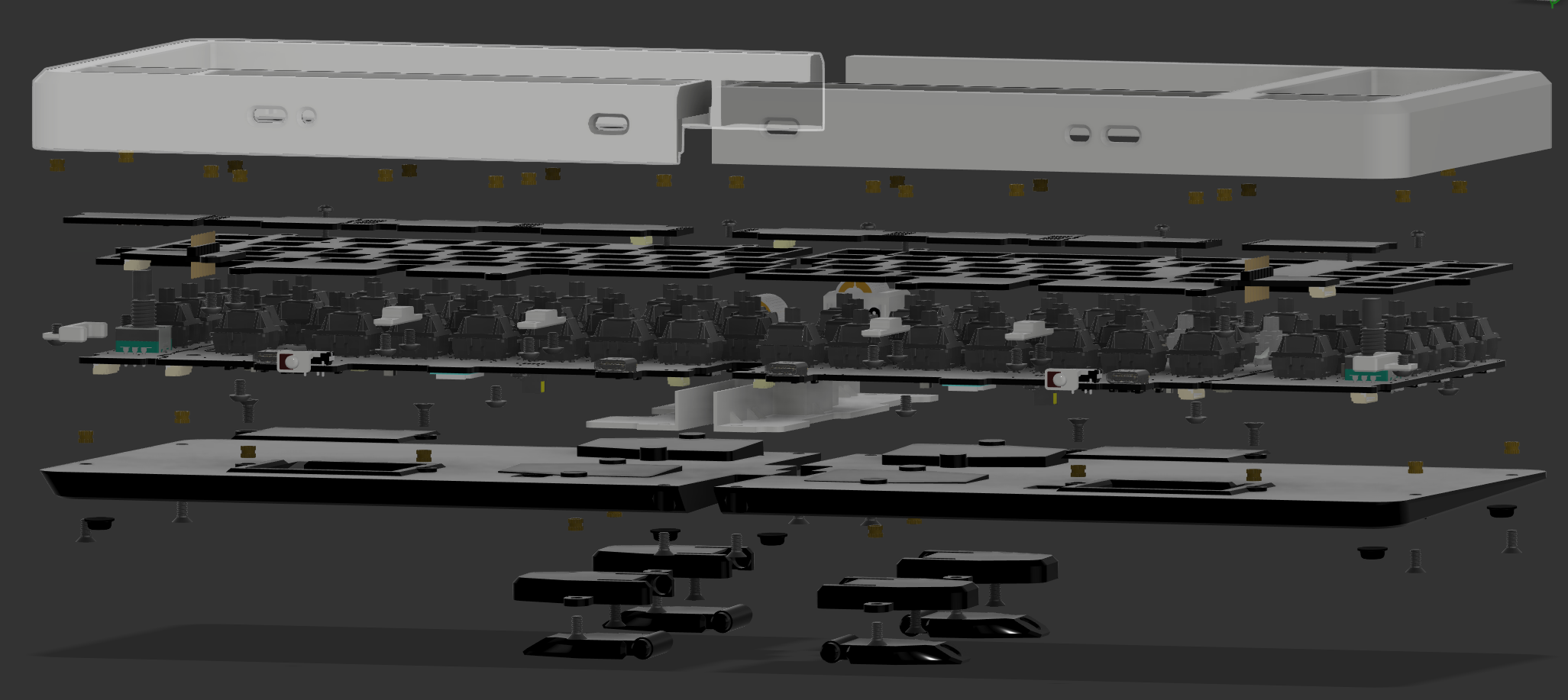
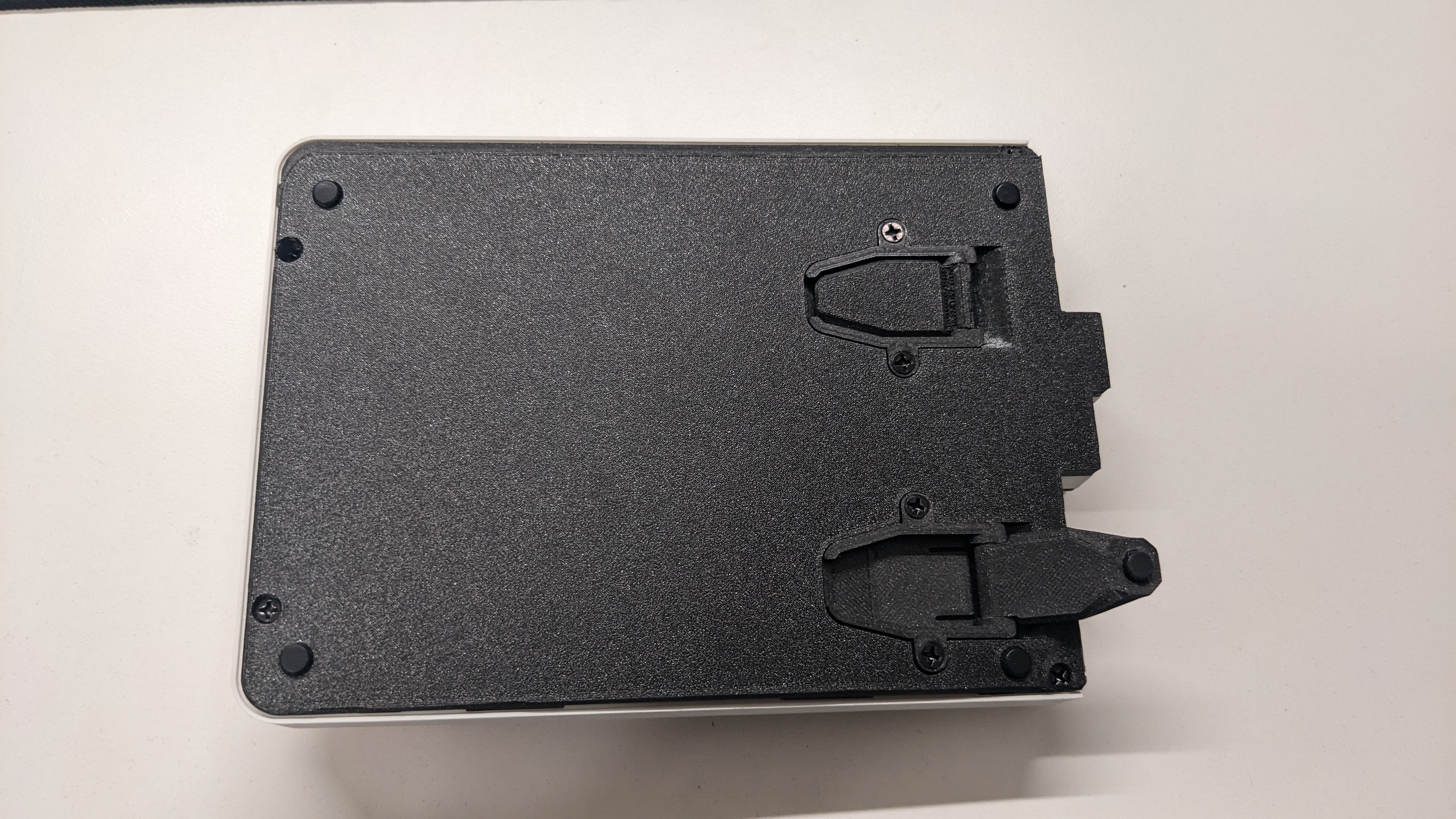
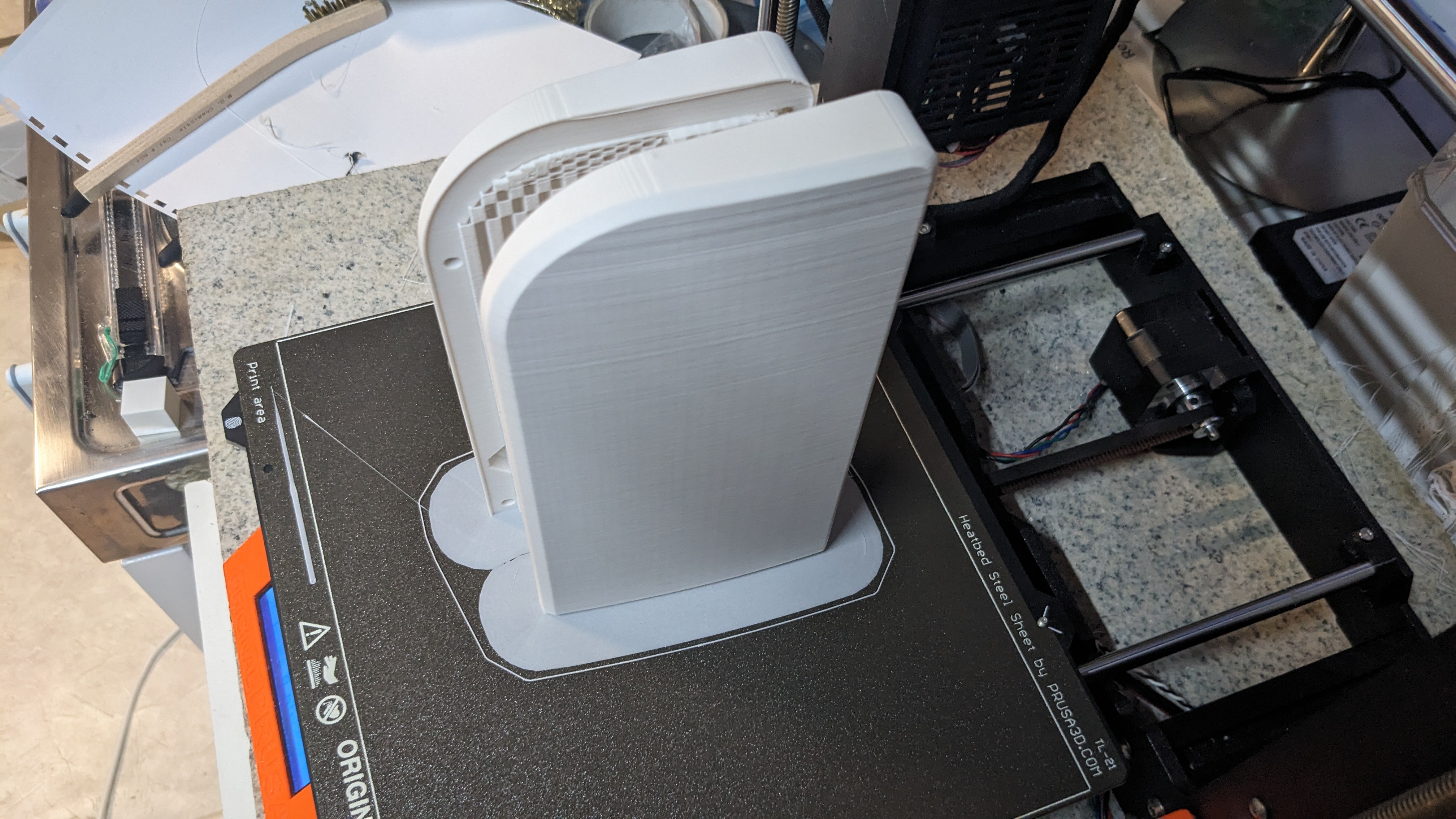
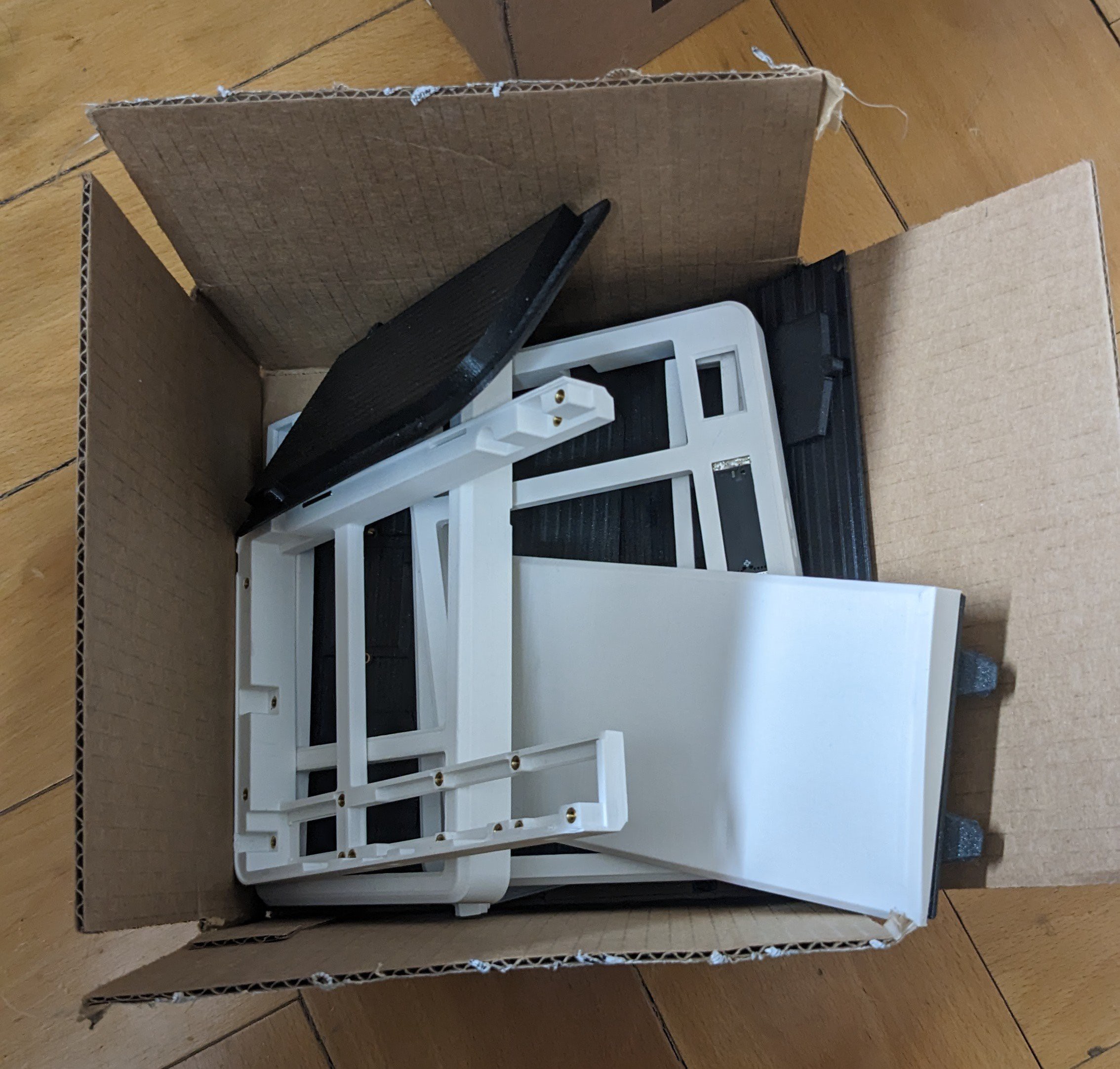
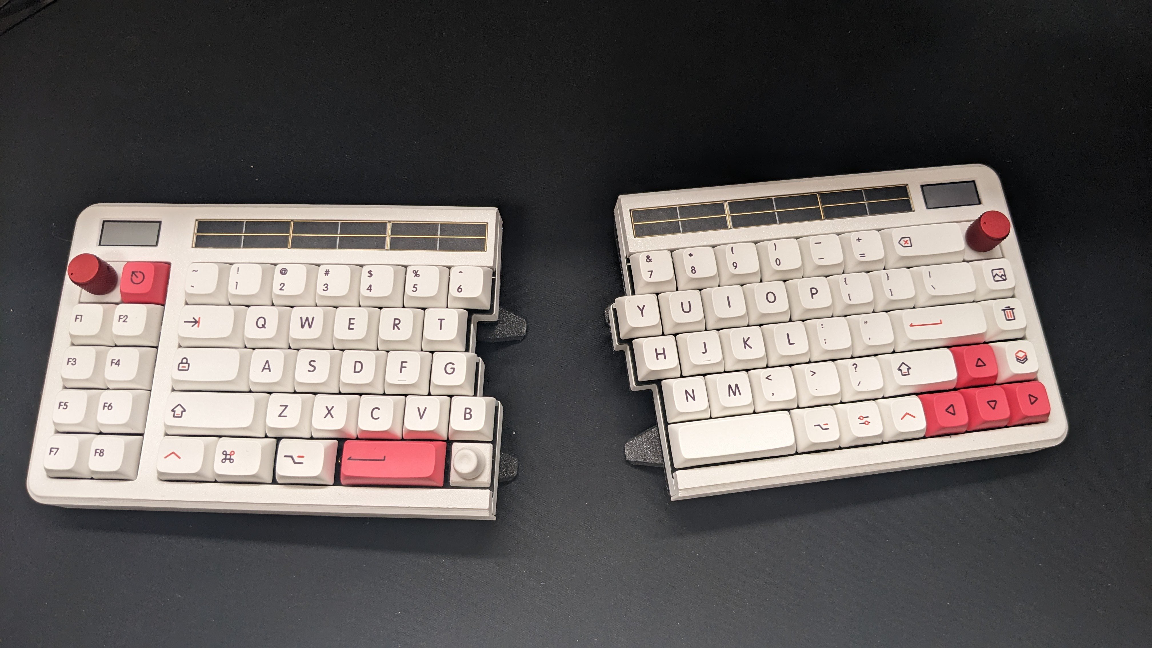
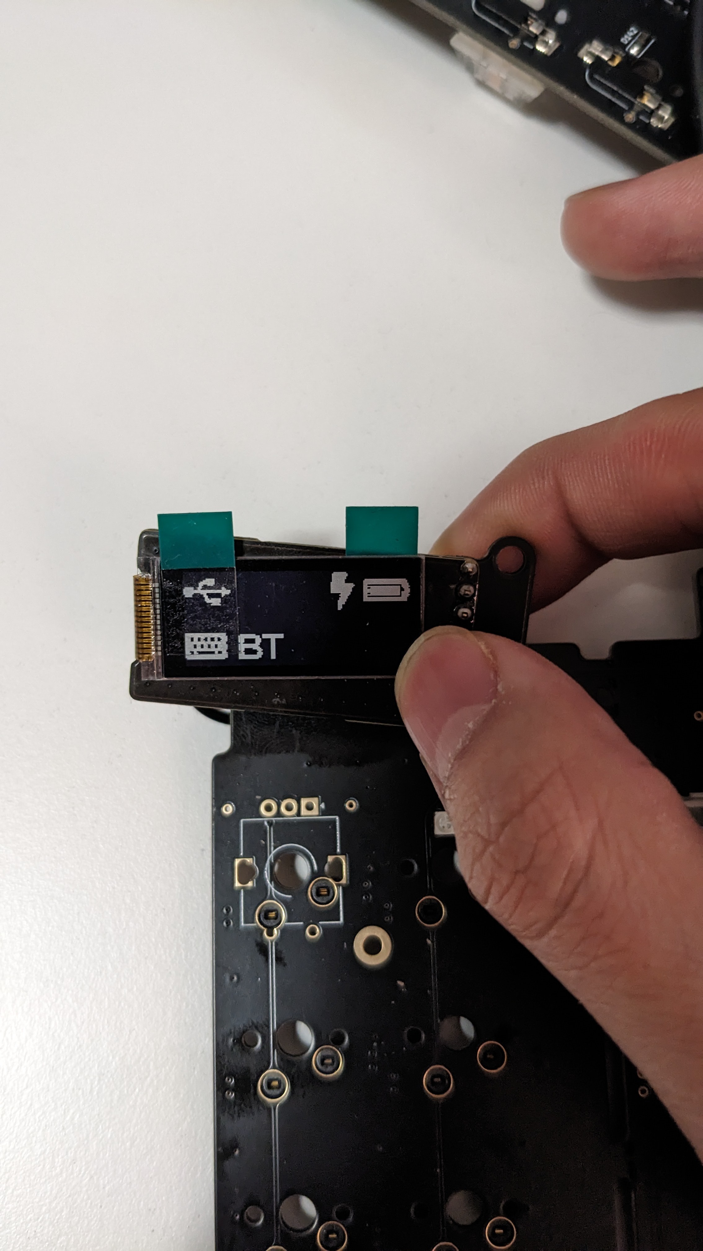
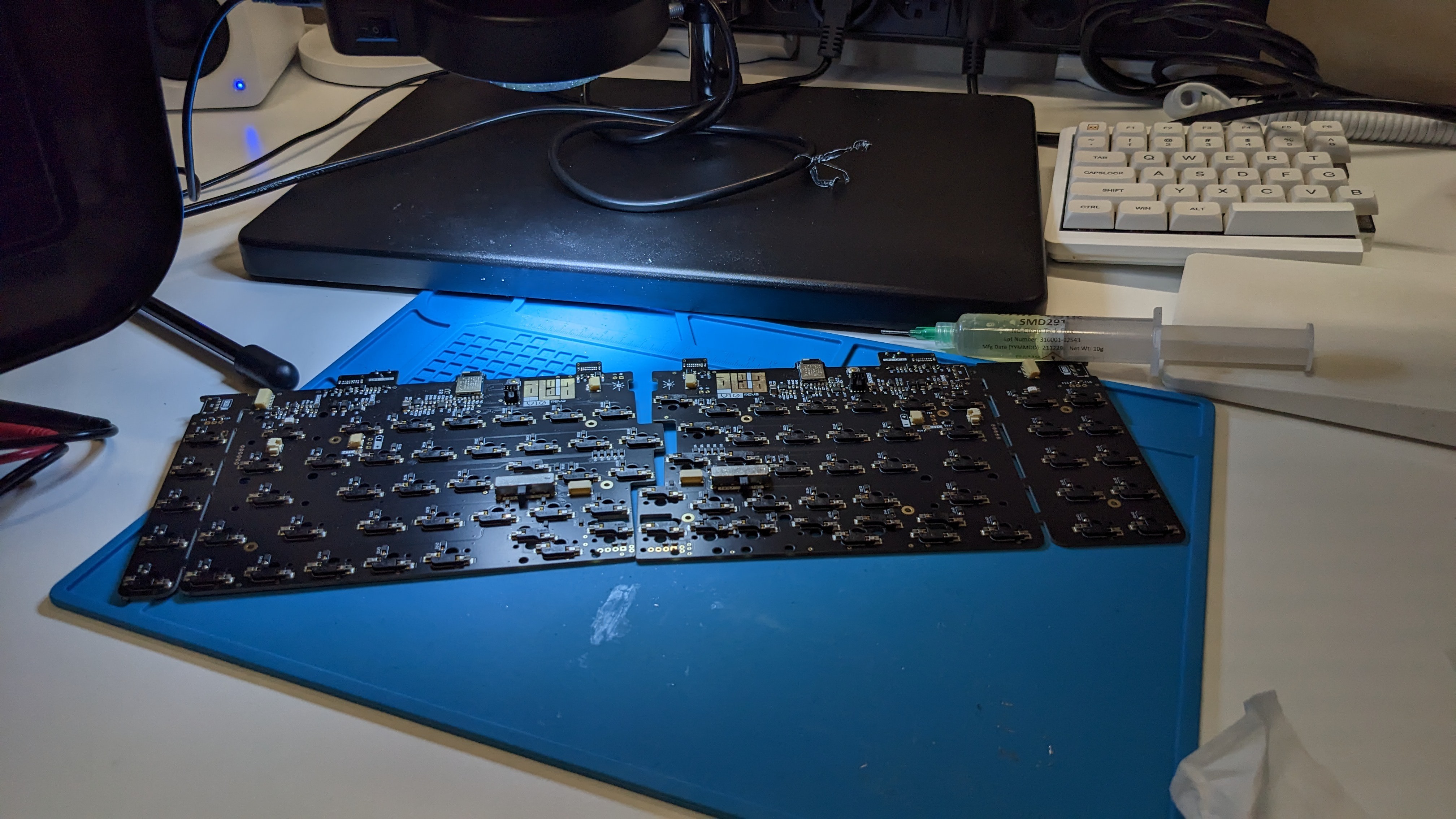
Aloidia: wireless split solar powered keyboard
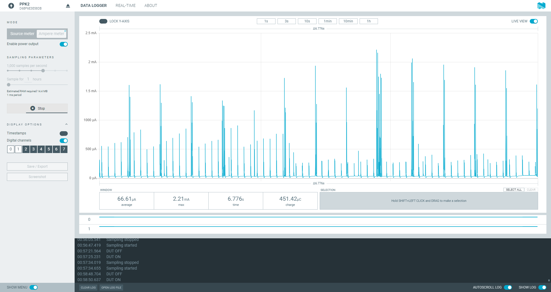
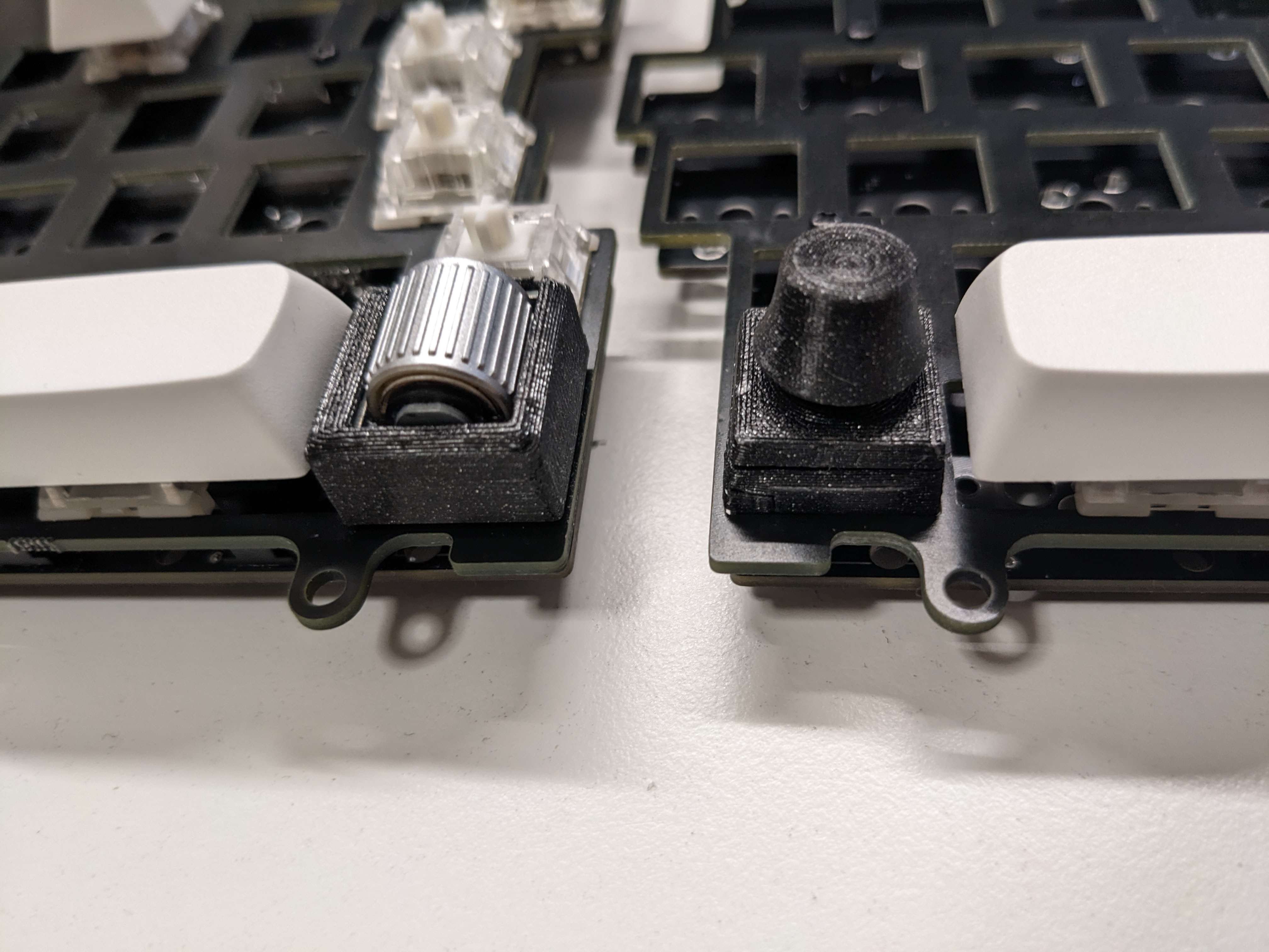
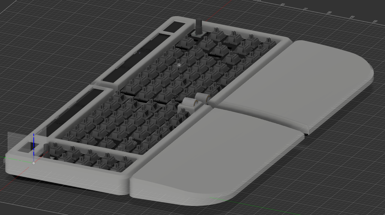
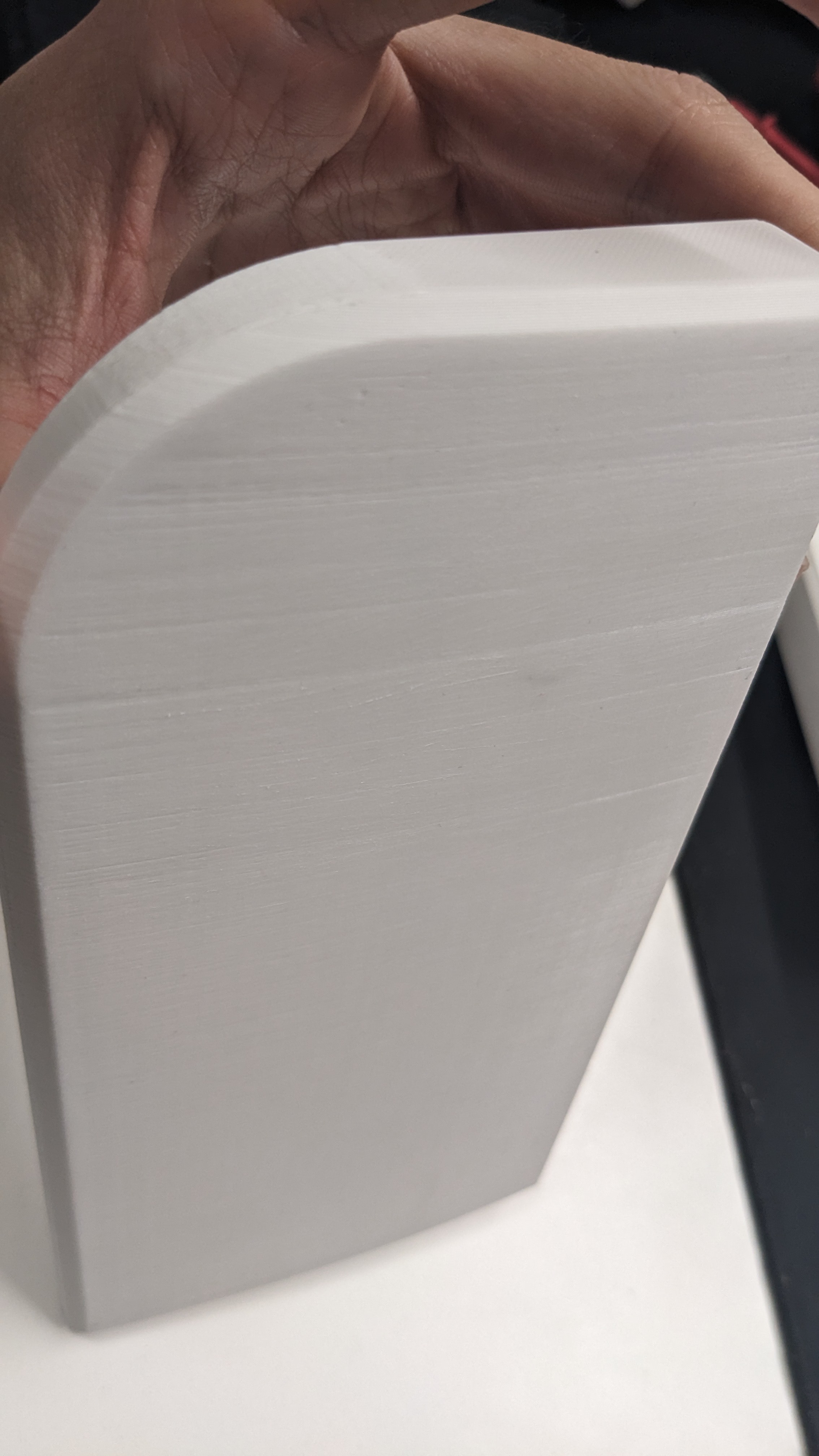
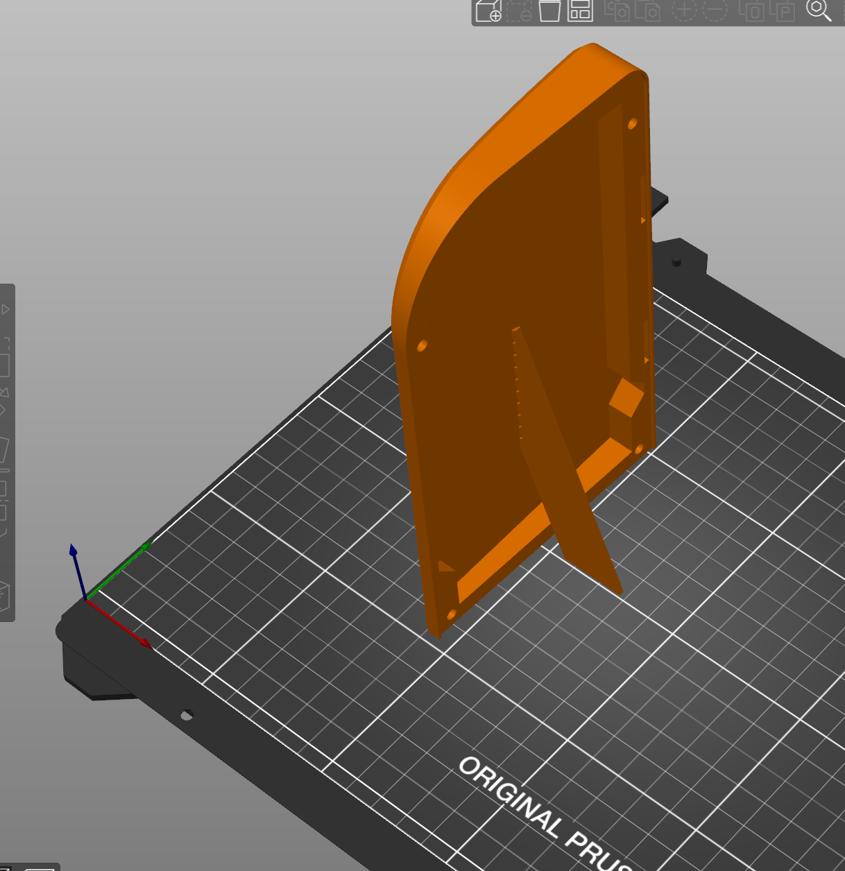
Aloidia is a staggered, split, fully wireless solar-powered mechanical keyboard with extremely long battery life.
 Nguyen Vincent
Become a Hackaday.io member
Already have an account? Log in.
Just one more thing
To make the experience fit your profile, pick a username and tell us what interests you.
Pick an awesome username
hackaday.io/
Your profile's URL: hackaday.io/username. Max 25 alphanumeric characters.
Pick a few interests
Projects that share your interests
People that share your interests


 mkdxdx
 Mattia Dal Ben
 Bulbul
Oh myyy, this is a beautiful keyboard. Told myself I was semi-done with this hobby (more-so just focus on customising my already bought keebs and not joining anymore GBs), but if this becomes a group buy....I'm 100% in. Awesome work! Wish I was knowledgeable enough in electronics to create my own keeb this complicated :D