I started this near the end of December 2022.
Zbigniew Stachniac, at York University in Toronto, created an MCM/70 emulator which runs the actual machine code from an MCM/70 and which does an excellent job of emulating the experience of using an MCM/70. Looking through my correspondence with Zbigniew got me thinking about the development of the MCM/70. That involved the "rack" machine which was a hand built, wire-wrapped version of the MCM/70 with RAM in place of PROMs. Which got me thinking that it would be fun to build a replica of the rack machine using an actual 8008-1 chip and the necessary hardware to make it go. The goal isn't to make a clone of the old rack machine, that would be way beyond my level of ambition, just to make a machine that is electrically similar, connects to similar or identical peripherals, and could thus be used much like the original rack machine. This is not a small project.
So here is a photo - direct from the 1970's - of a very young me sitting in the machine room, with the original rack machine to my left.
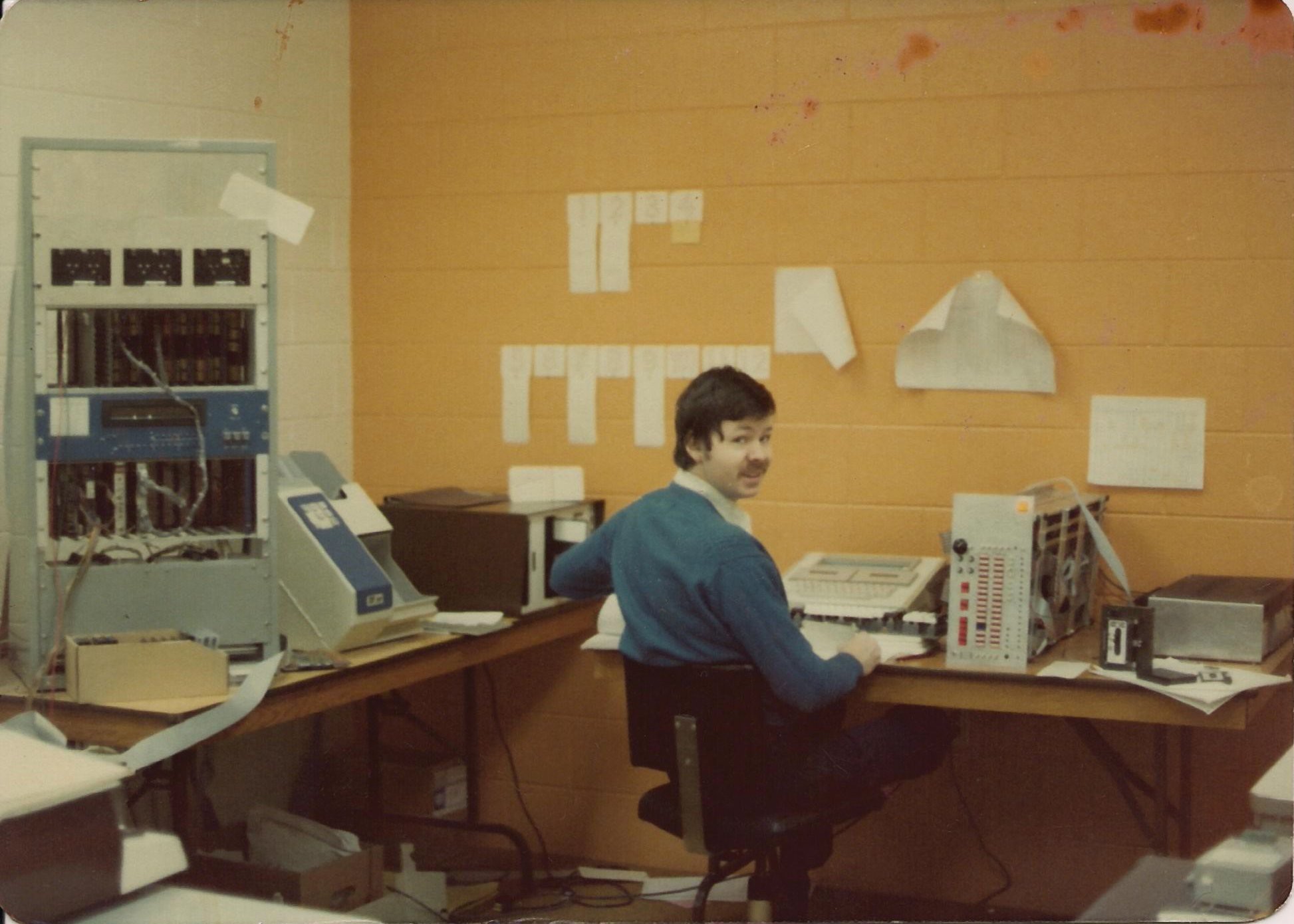
Top to bottom we have:
- A row of three MFE-250 digital cassette tape drives.
- A row of wire-wrapped card, probably mostly RAM. It took 64 2102 RAM chips (1K x 1) to make 8K bytes and the machine had around 44K. That's a lot of chips and wire-wrapping.
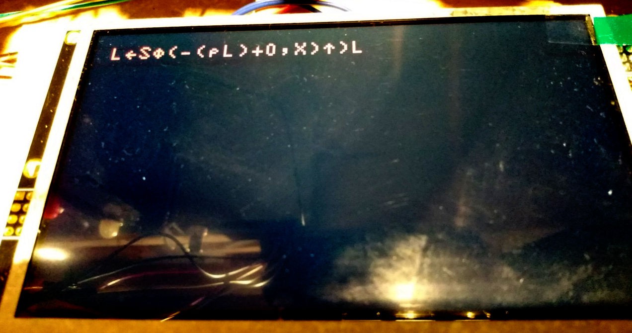
- A blue panel with a Burroughs SelfScan display (32 x 1), a white reset switch, three push buttons (no idea what they did) and some LEDs, barely visible, to display the address and data lines.
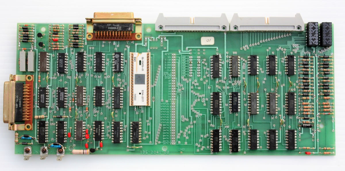
- More wrie-wrap cards, mostly interface cards to the peripherals.
- A gray panel with the power supply.
- A cardboard box full of digital cassette tapes.
To the right of the machine is a punched card reader. Yup, back in the day all the programs were done on punched cards and all the programmers time shared the one IBM 029 keypunch machine in the office. To the left of the rack machine, not shown in the photo, is a Diablo HyType daisy wheel printer and a keyboard.
A brief introduction to the architecture of the MCM/70
The 8008 has only 14 address bits, allowing it to address 16K of memory. That wasn't enough for what MCM was trying to do, which was to build a personal computer that ran the APL language. The solution was bank switching. So, in a production MCM/70, the memory space was laid out thus:
- First 6K: startup code and commonly used routines.
- Next 2K: 16 banks, any one of which could be in use a time, and selected by an I/O command.
- High 8K: Ram for the users APL workspace.
In the rack machine the low 2K was 1702 EPROMS while the rest was RAM. What was in the EPROMS was the low 2K of the APL interpreter along with a little rinky-dink loader which could read object code from a tape and branch to it. After that you were on your own.
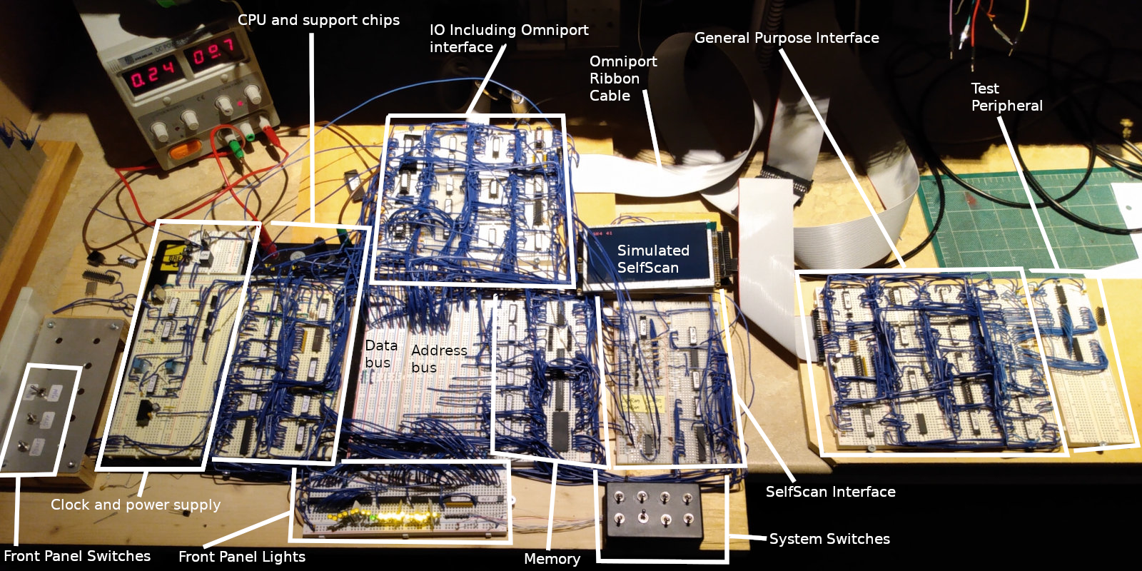
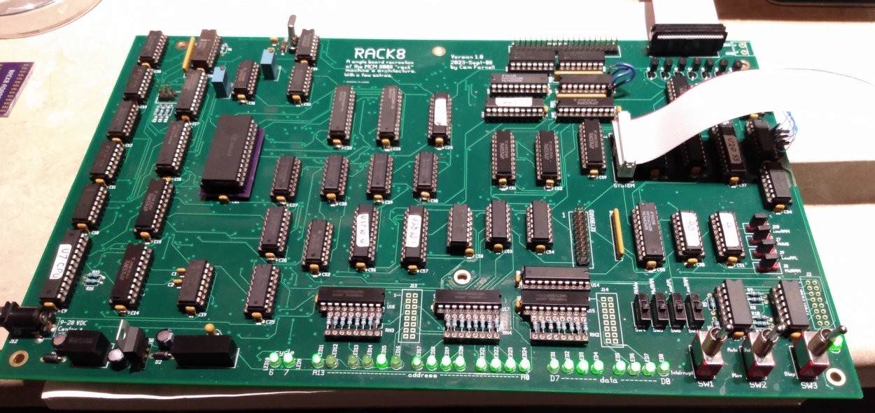
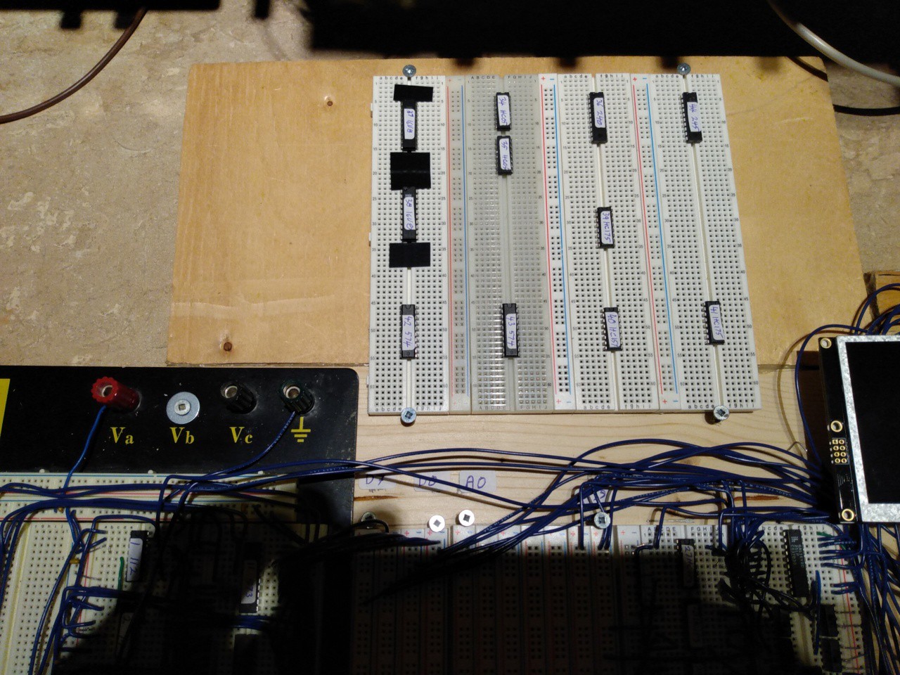
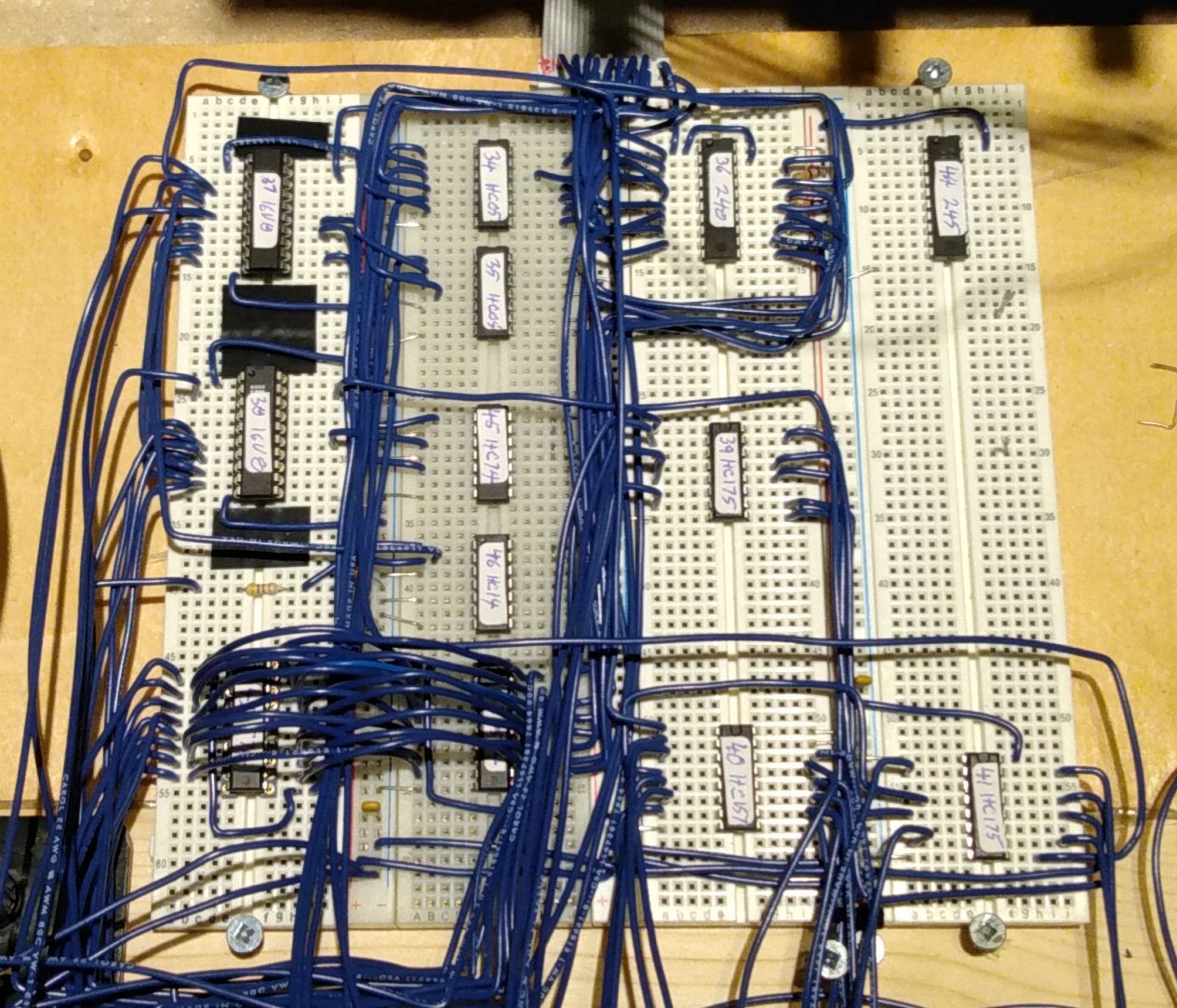
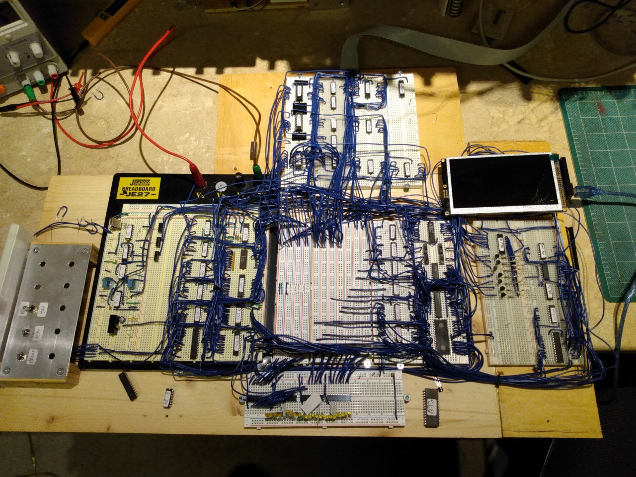
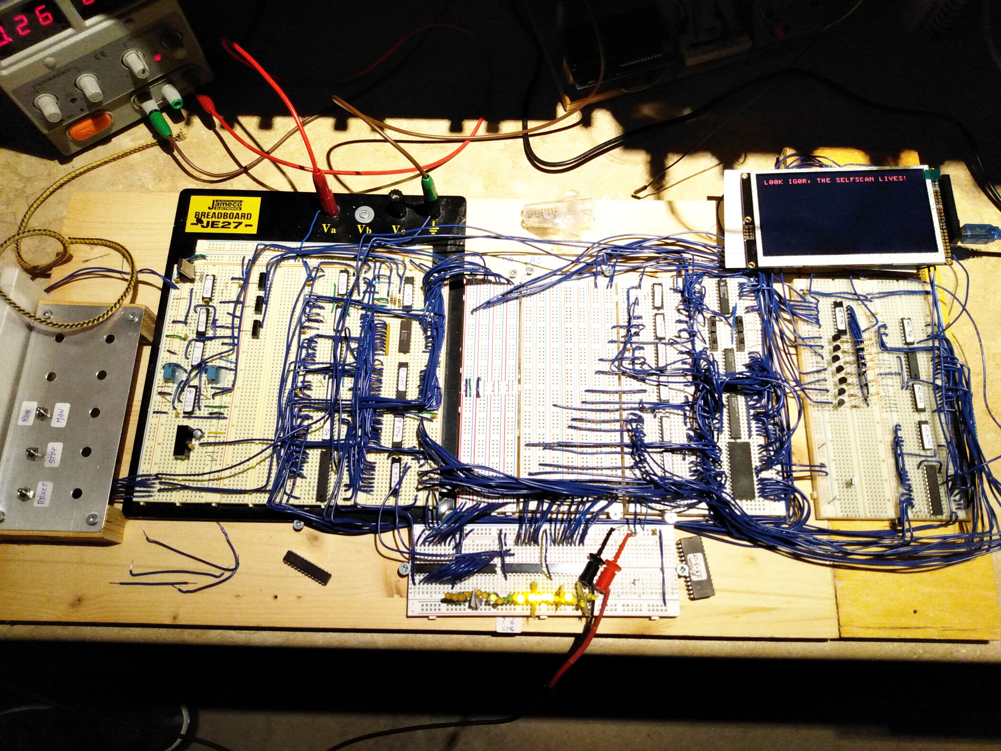
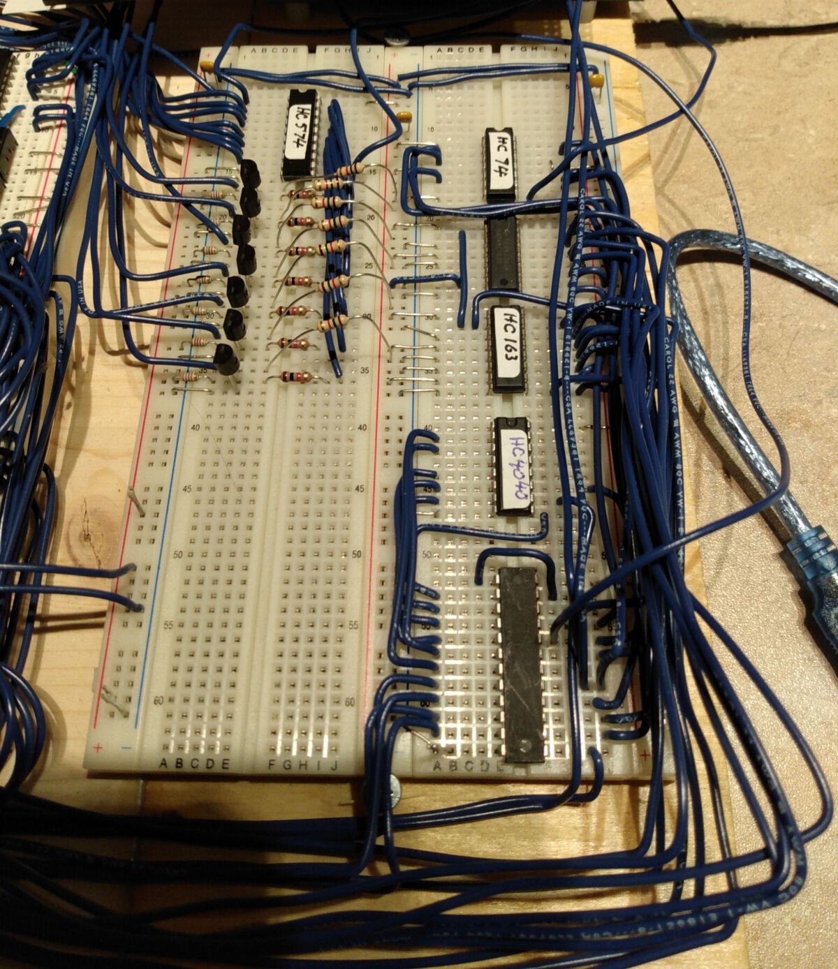
A brief introduction to the Rack8 replica
The goal for the Rack8 is to have a machine which is functionally the same or very similar to the MCM rack machine. Toward that end it should have these characteristics:
- An Intel 8008-1 CPU
- EPROM or RAM (selectable) memory for the first 2K from X'0000' to X'07FF'.
- EPROM or RAM (selectable) memory for the next 6K from X'0800' to X'17FF'.
- EPROM or RAM (selectable) memory with 16 2K banks at address X'1800' - X'1FFF'.
- RAM memory for the last 8K X'2000; - X'3FFF'
- LED's that display the data and address busses.
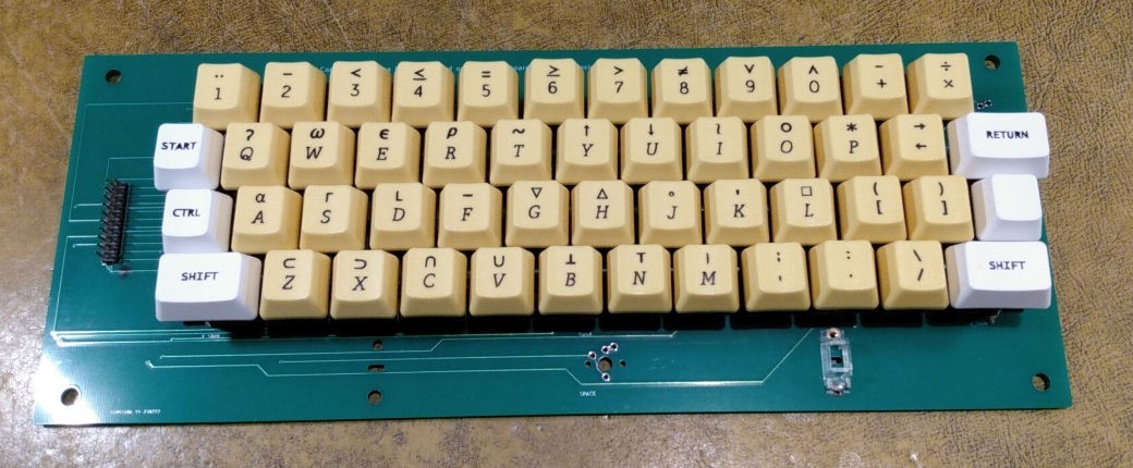
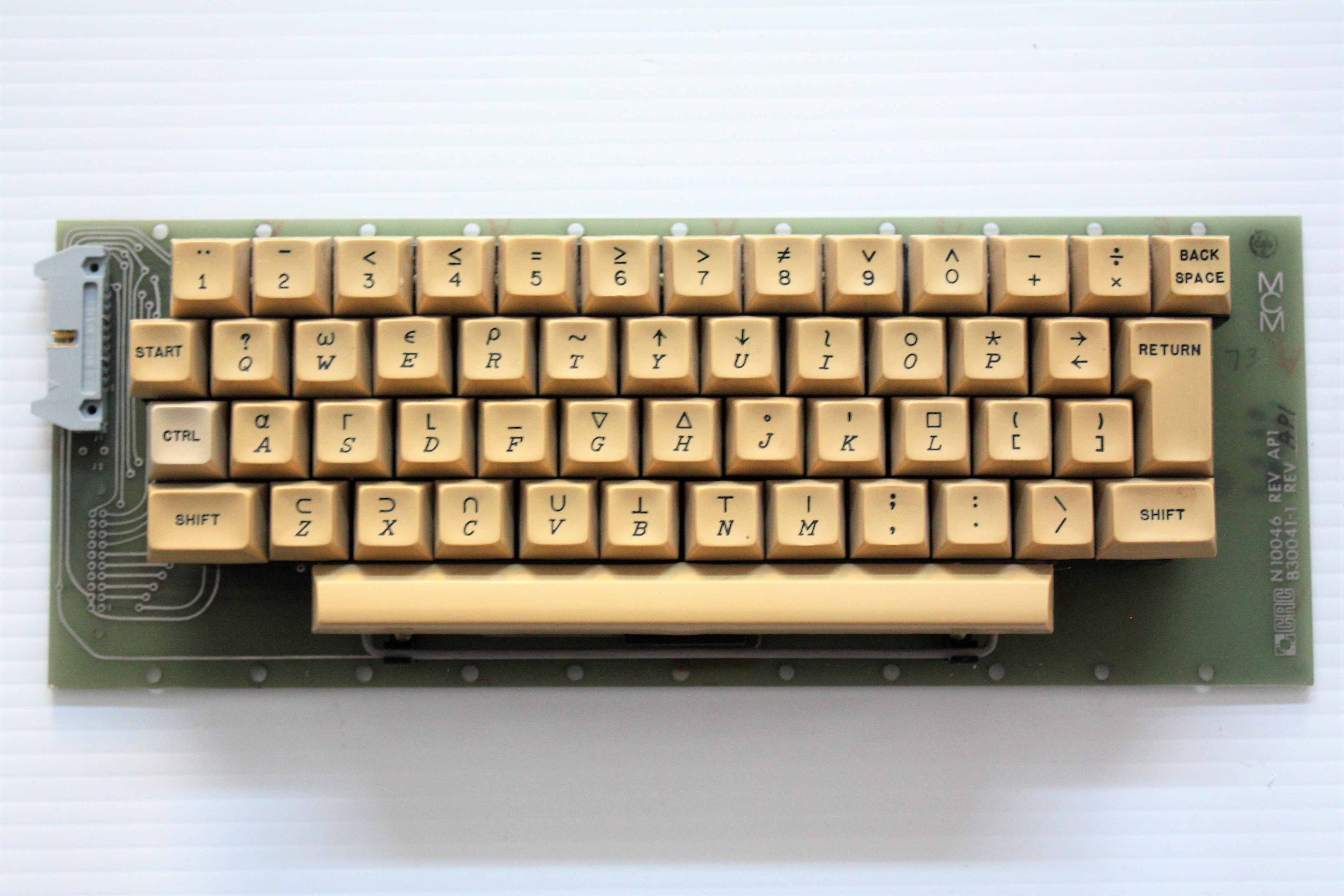
- A keyboard connector that is plug-compatible with an MCM/70 keyboard.
- A display connector that is plug-compatible with a Burroughs SSD1000-0039 Self-Scan plasma display.
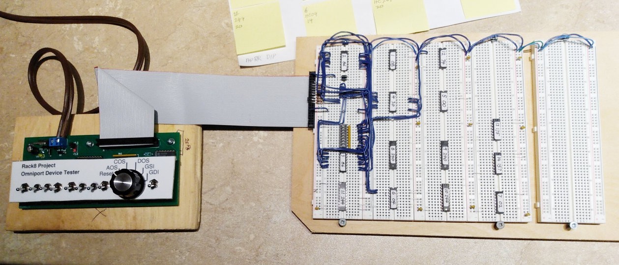
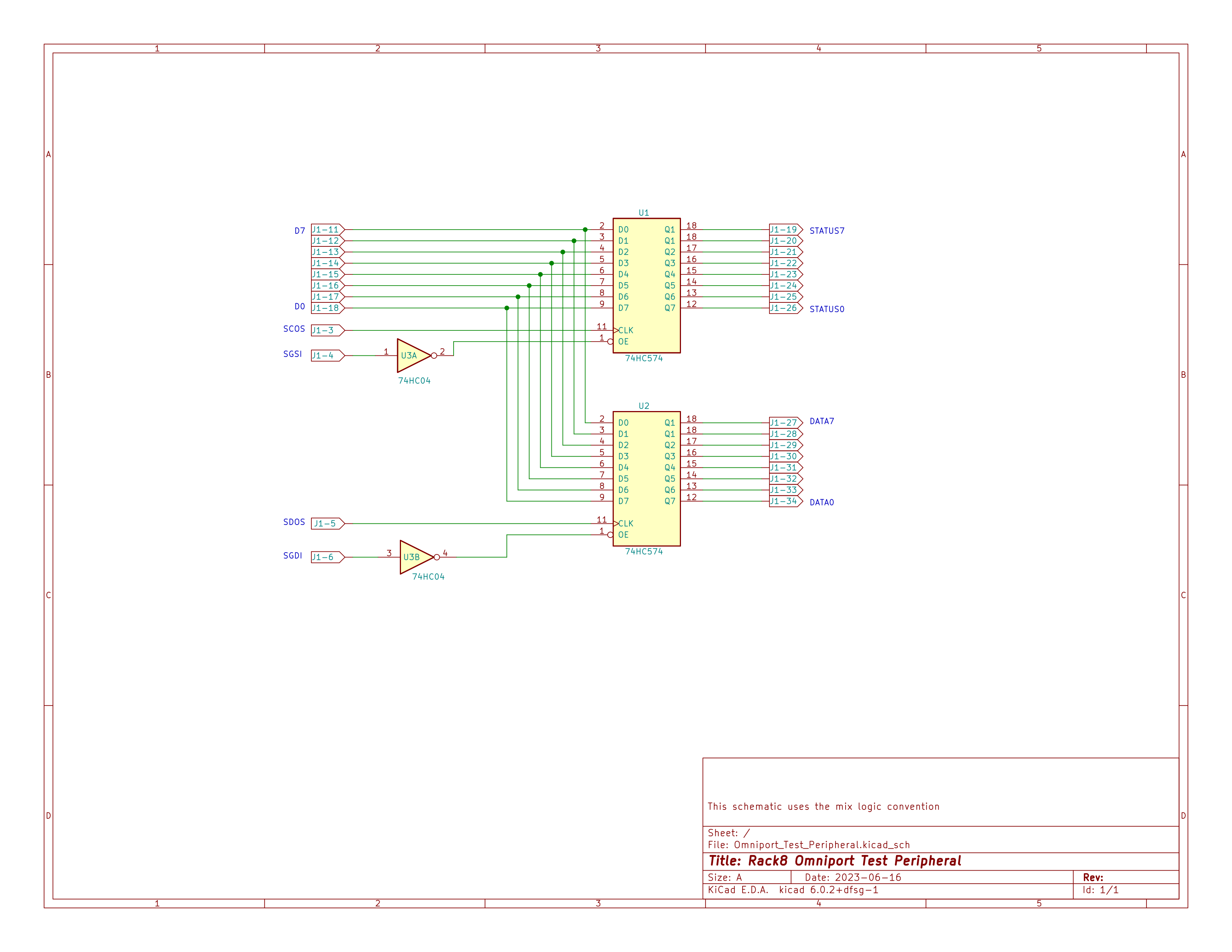
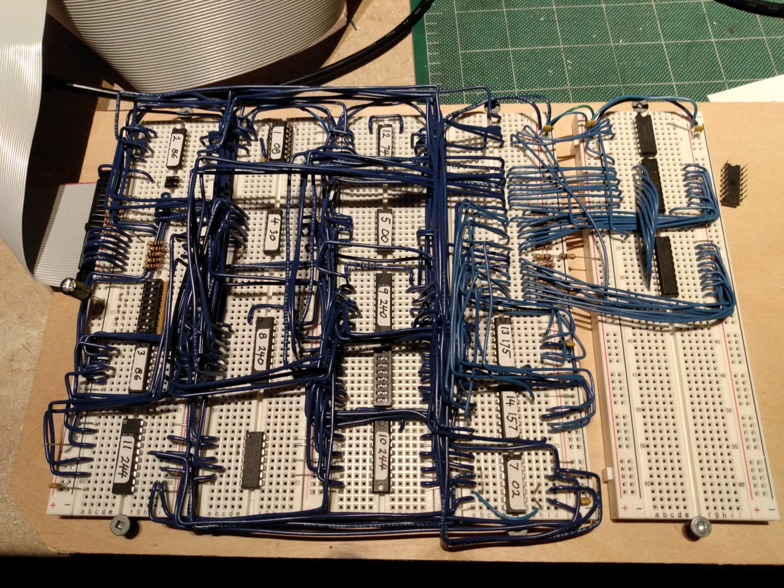
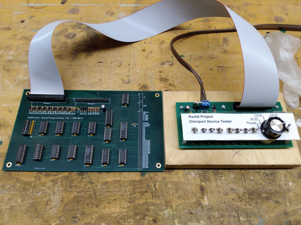
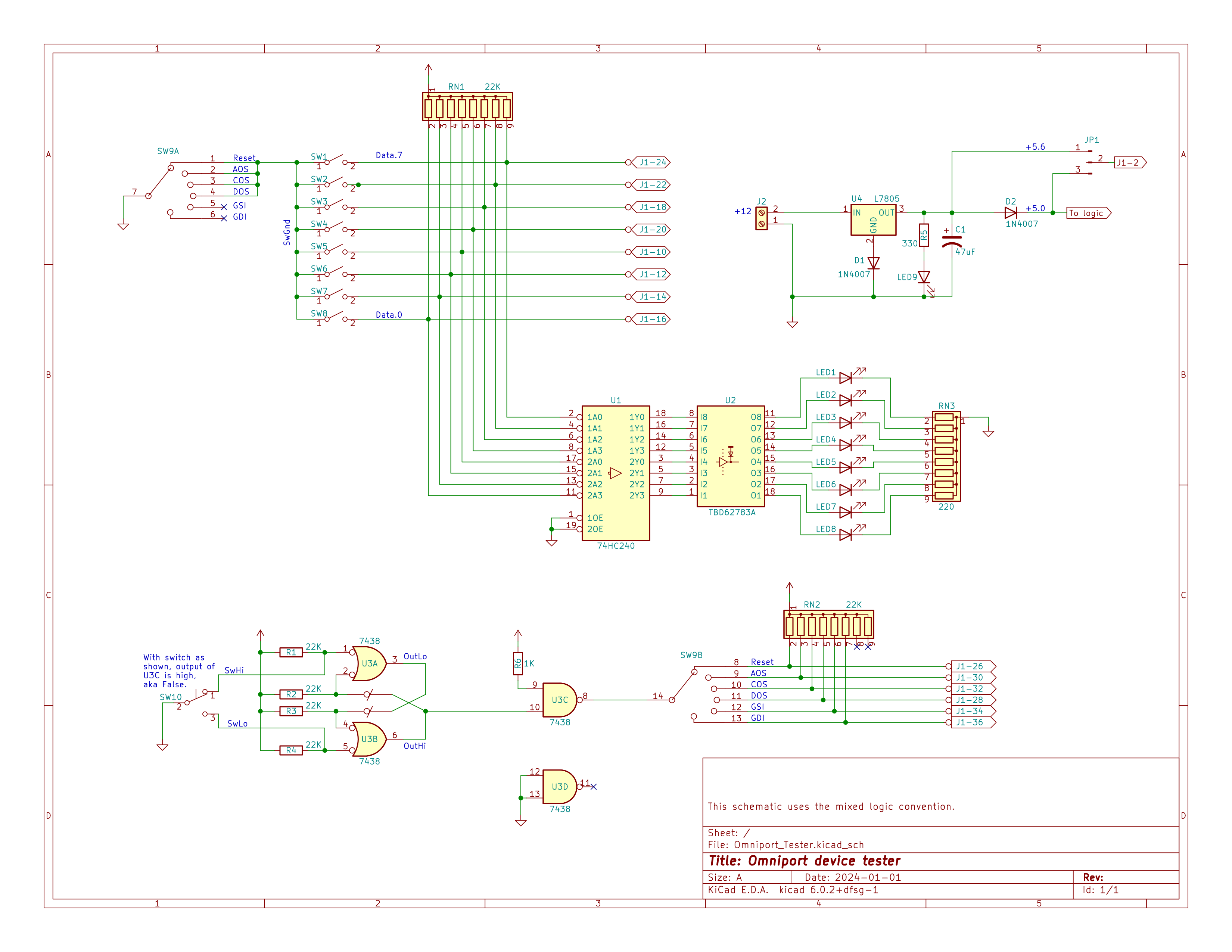
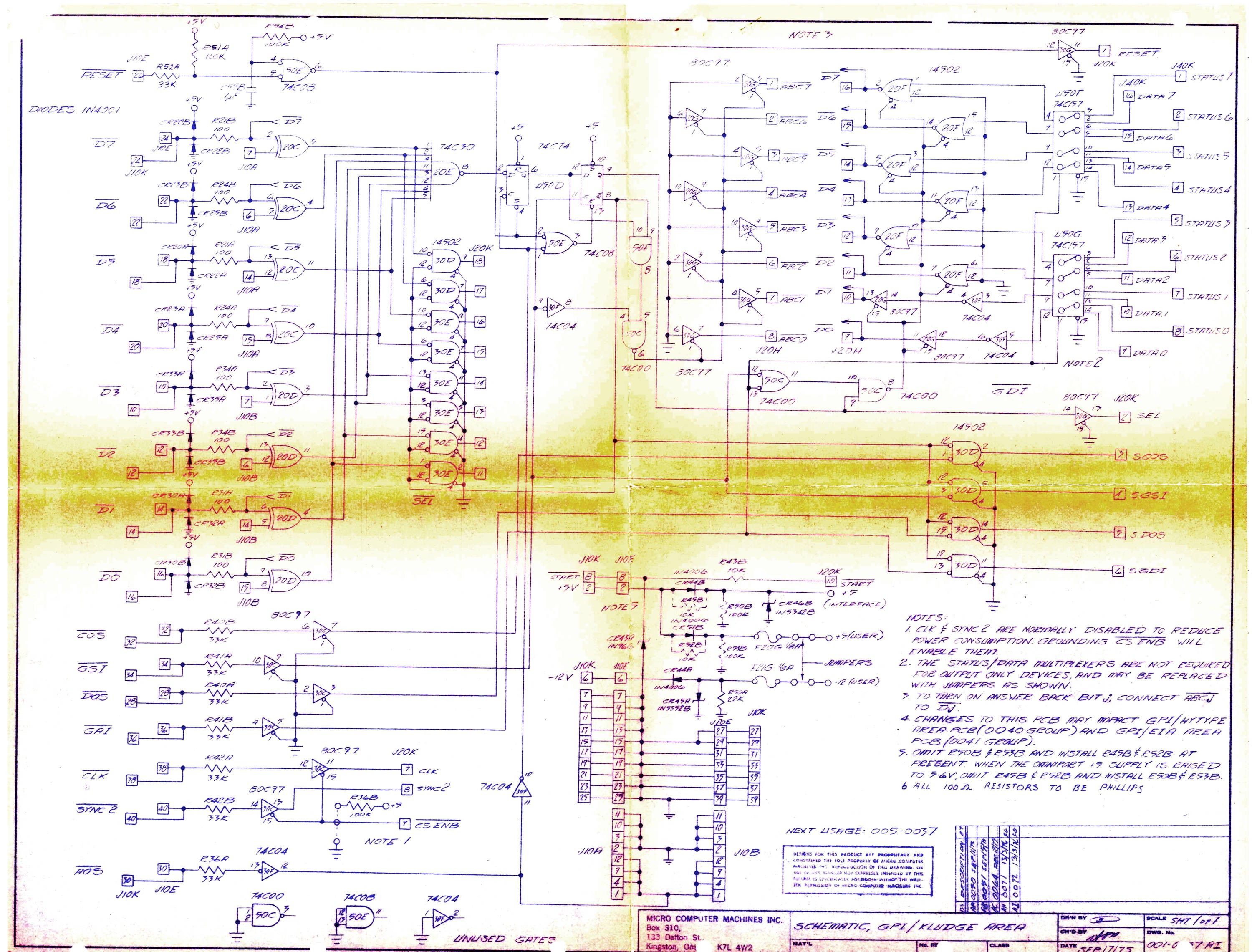
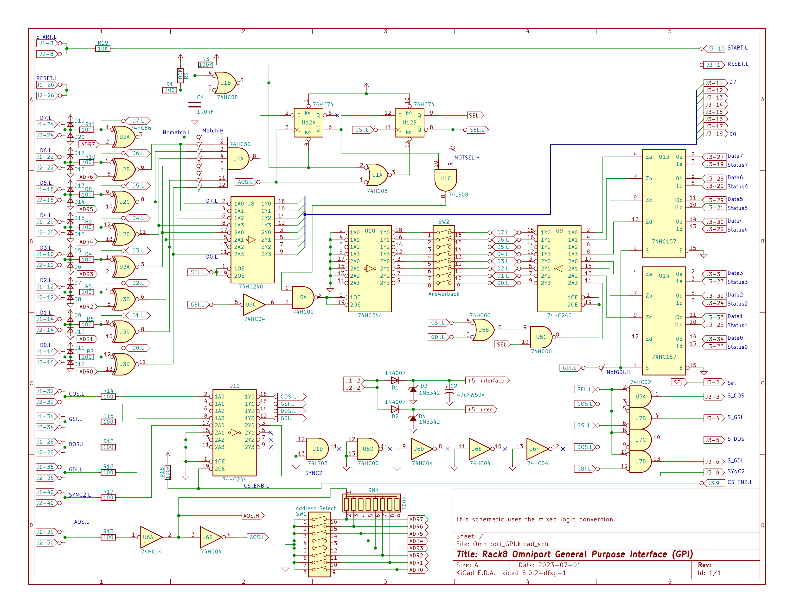
- An "omniport" connector, for connection to MCM compatible peripherals, that is electrically and physically the same as the omniport connector on an MCM/70.
- Two connectors, each of which can connect to an MFE-250 digital cassette drive.
- Be a single-board computer of modest size.
Some challenges
Some things are more available than others. Intel 8008-1 CPU's are still available on eBay. I've got enough RAM and EPROMS in my parts drawers. A keyboard can be made. But Burroughs Self-Scans and...
Read more »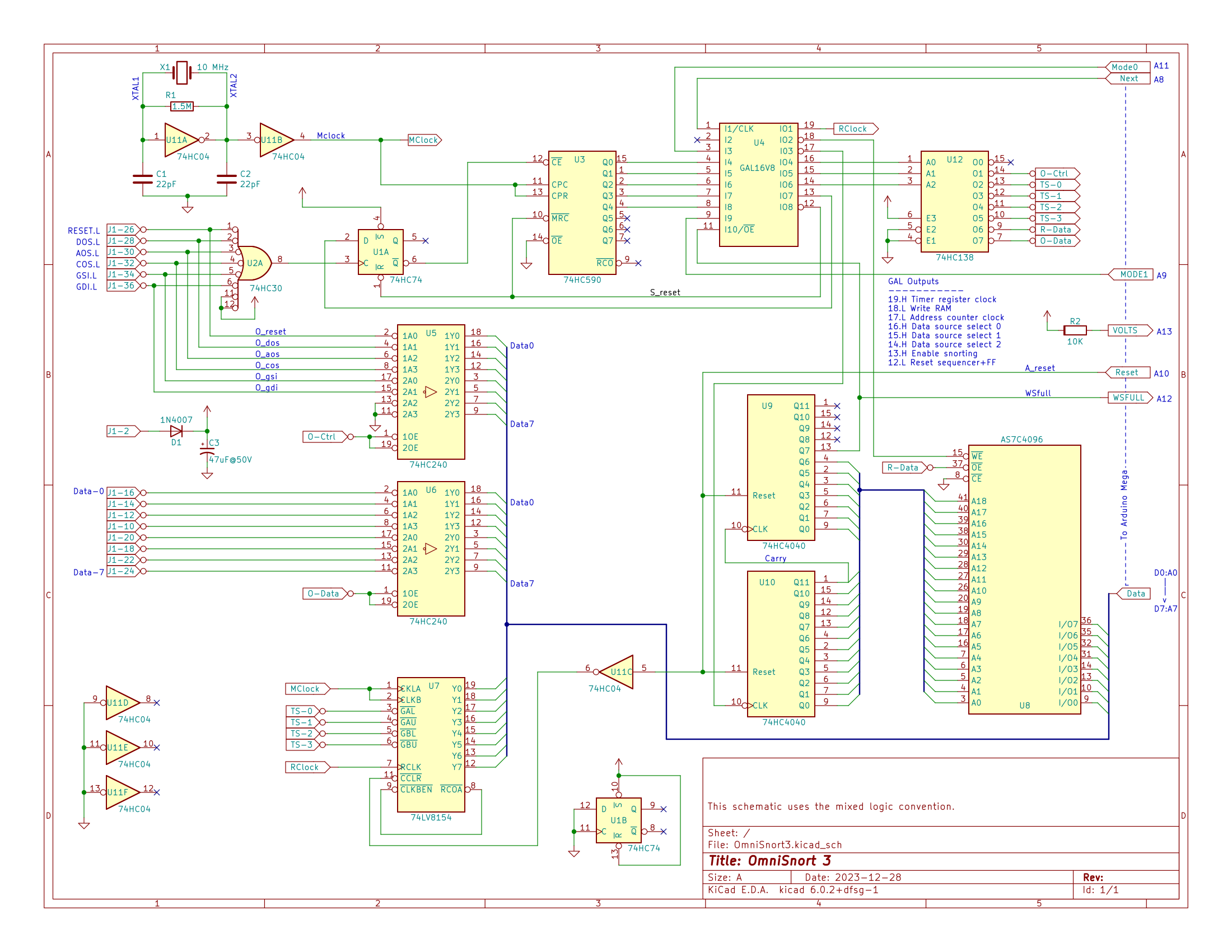

 teardownit
 Benchoff
 Maarten Janssen
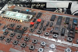
 Keri Szafir