 Keri Szafir
The Sochor DRX85 is a complex device consisting of input and output preamplifiers, analog-to-digital and three digital-to-analog converters, mode/function selection switches and circuits, time circuits (haha), power supply, level meter and the most important part: the RAM chip based delay line where data is stored in a cell at a time, and then read from this cell after the delay time has passed. The device uses three 64kbit RAM chips, so it can store 192kbit of data at a delay time of up to 1280ms. The memory board was designed with more than just three chips in mind and works by daisy-chaining them, though I'm not sure if there was a version of the device that actually used more than three (the design minimum). There is no existing data or schematics on the web, apart from what I found out by reverse-engineering.
First, let's take a look at the high-level design, block diagram:
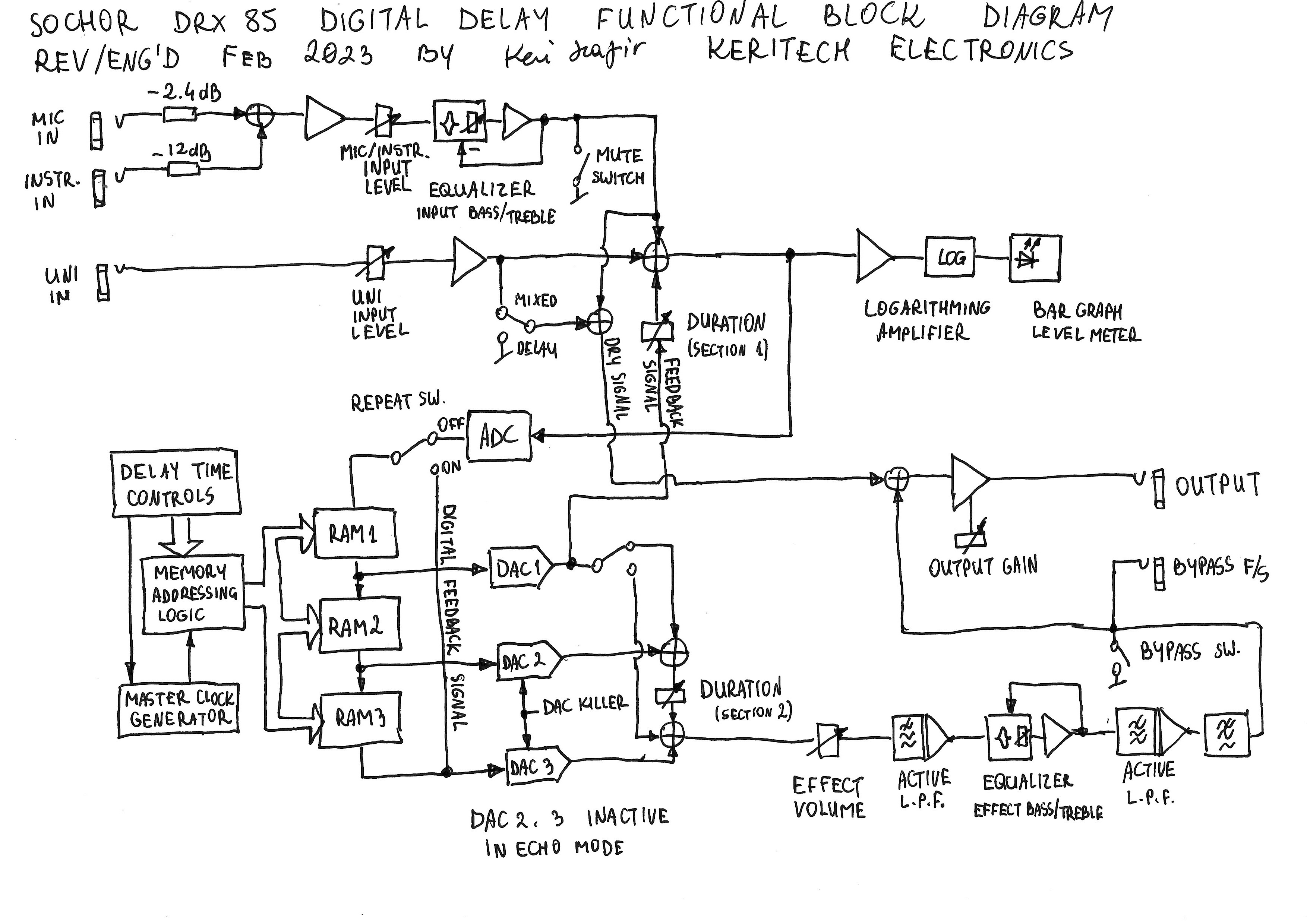
The mic and instrumental inputs pass through a preamp with volume and tone controls on the front panel, whereas the universal input with a level adjustment pot on the back has a feature the others don't: it can be delayed without mixing with the dry signal. Probably meant for effect send/return loops in mixers, where you can adjust the proportions between dry and wet on the mixer rather than on the effect device. The "bypass" switch doesn't bypass the effect - it just shorts the wet signal to ground, allowing dry only.
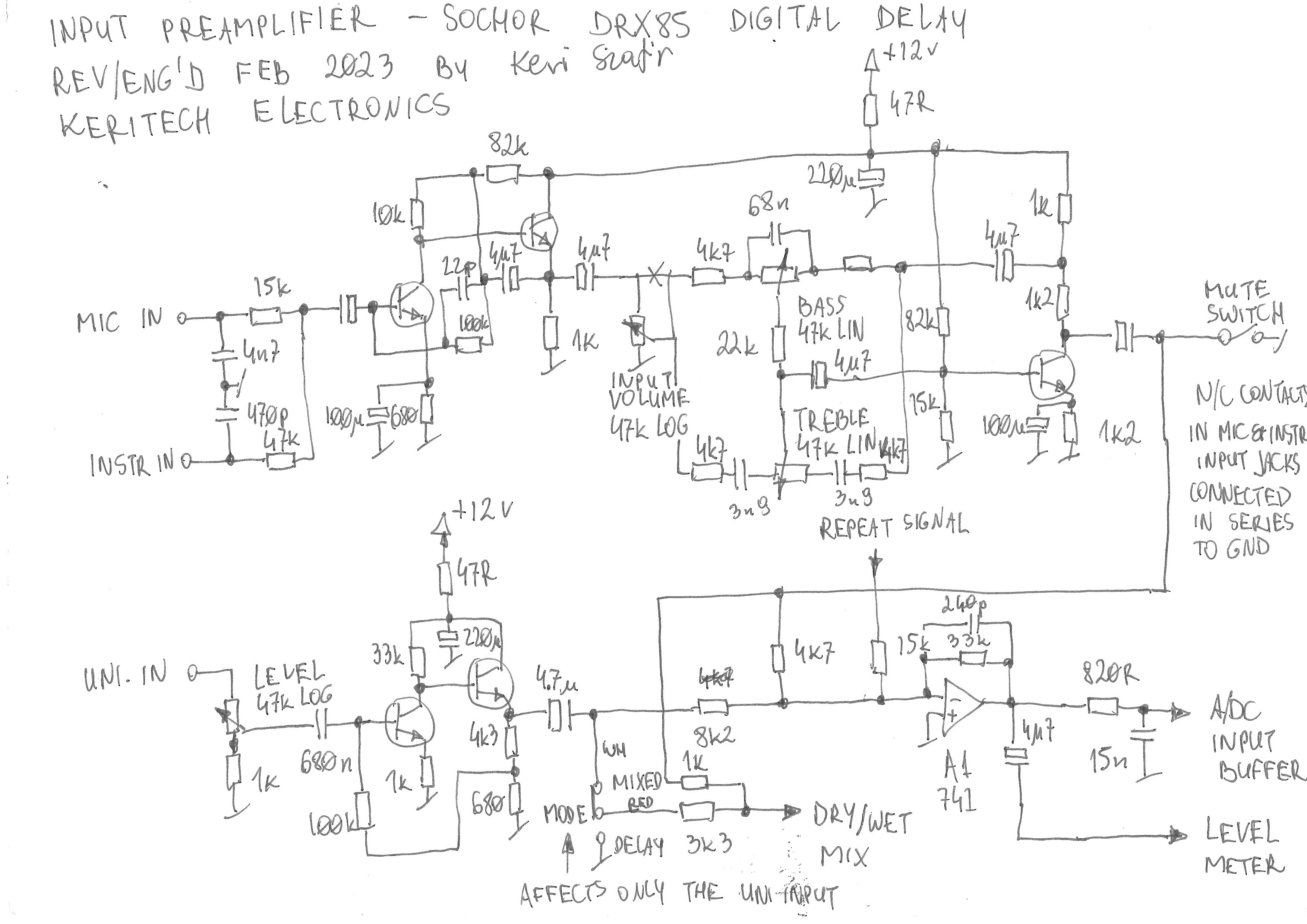
It's interesting that the input preamplifier - apart from the stage feeding the meter and ADC buffer - is built entirely with discrete transistors rather than 741 opamps. It also tells volumes about the IC market in mid `80s here; no TL072, JRC4558 etc. lower noise chips. The tone controls are classic active Baxandall type.
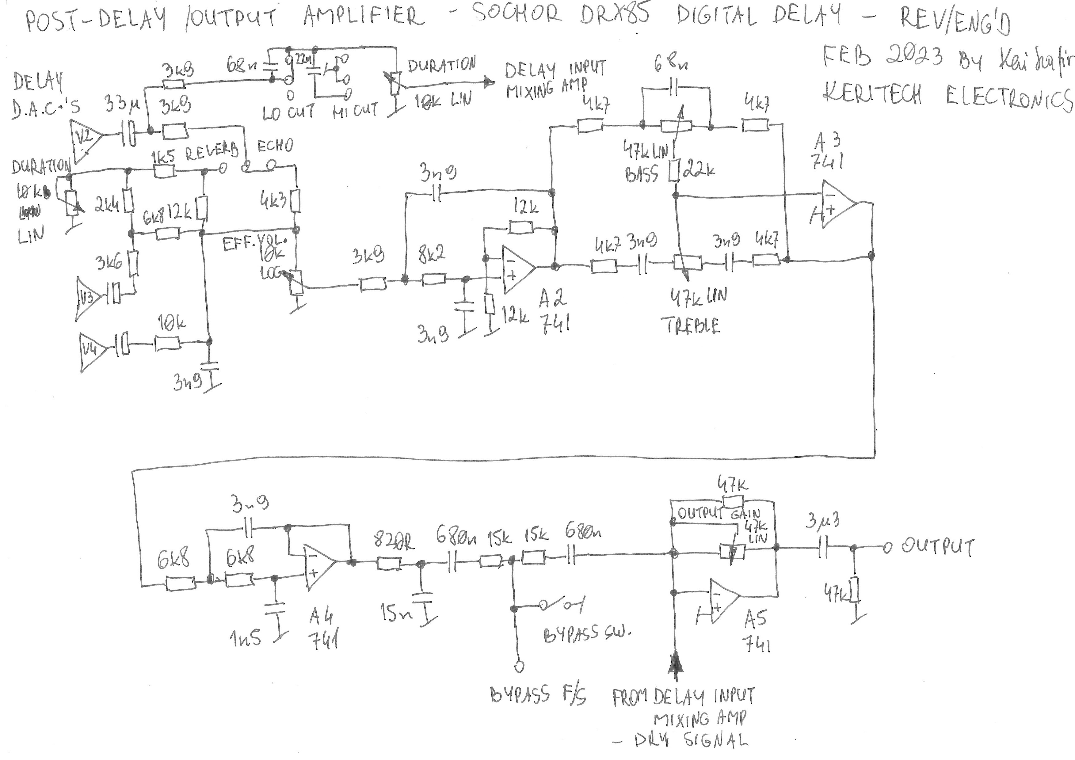
Post-delay circuit is mainly DAC mixing (where the 2nd and 3rd DAC which I marked V3 and V4 is active only in the "reverb" mode), two Sallen-Key type active low-pass filters, between which we can see an even more classic op-amp based active Baxandall tone controls. Then some passive LPF and a bypass switch and footswitch that shorts the wet signal to ground. Then the dry/wet mixing node and final opamp with output gain adjustment.
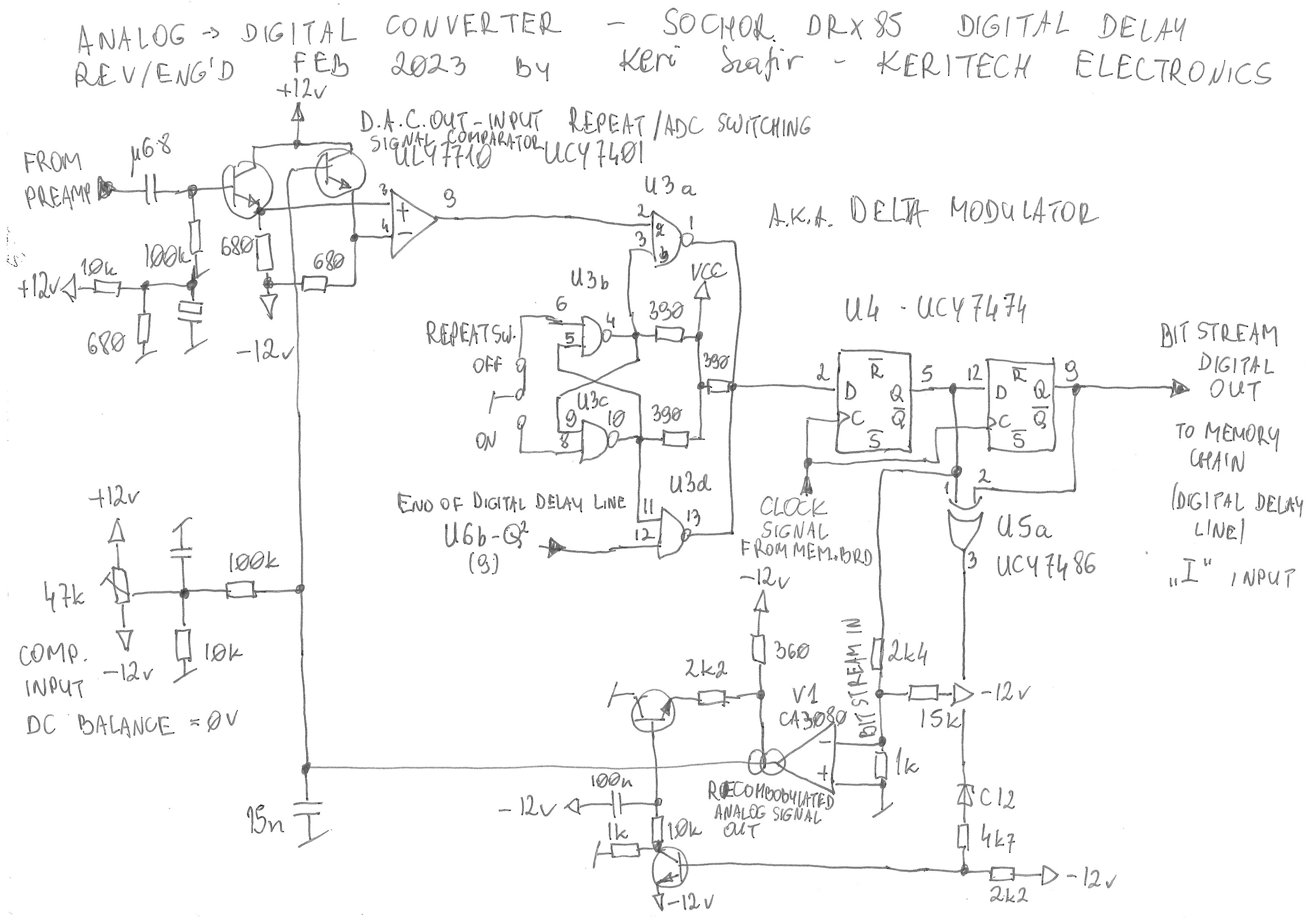
And now the interesting part. I'm not that great when it comes to understanding the analog-to-digital converters, but this is a delta or delta-sigma converter with an added signal selection circuit which switches between ADC and looped digital signal circulating around the delay line. The analog signal is fed through a transistor buffer to a positive input of a comparator (ULY7710) which checks the voltage difference and outputs logical 1 when input voltage is higher or 0 when it's lower than the output of a DAC in the feedback loop. The digital signal is fed through the selector into the D flip-flops which both gate the signal on the output of the selector at a clock pulse and detect whether the new bit on pin 5 is different than the previous bit stored on pin 9. If there's any difference, the new bit will make it through the CA3080 operational transconductance amplifier and be integrated into the voltage level on the 15nF capacitor. The voltage level will be fed through a buffer into the negative input of the comparator.
The potentiometer adjusts the DC level on the negative input of the comparator so that we can set the voltage difference to zero.

This is a digital-to-analog converter similar to the one in the ADC's feedback loop. Worth noting is the "blocking" diode: when the echo mode is selected, the second and third DAC have this pulled down to -12VDC, and thus the amplifier bias input is permanently at the lowest level, putting the operational transconductance amplifier out of action. When the "reverb" mode is selected, the blocking inputs of all DACs (1, 2 and 3) are ganged together and connected to the "DAC killer" circuit which temporarily pulls them down to -12V when a different delay time is being selected with a touch sensor. This prevents ugly glitches by muting the delayed signal altogether. I don't really know why it wasn't just muted in the analog domain with a JFET etc. but hey. Engineers have their quirks.

These are the time circuits! Last time departed, current time and destination time... Oh hey, I think I'm going too far. Anyway, the UL1958N chips are touch sensor selector ICs originally meant for voltage-controlled and varicap tuned radio receivers/tuners which were pretty trendy in the '70s and '80s. The IC's voltage selection is not actually used here, it's the latch and lamp driver that does all the job. An active channel's lamp output will be pulled down to GND and this sends a low level to an AND gate, setting the subsequent gates to output logical 0. The signals combined will just be a bunch of bits on a parallel interface. So, first delay time option (5ms) will output 0, 10ms will output 1 (big endian), 20ms will output 3 etc. all the way to 640ms which will output 127. These signals control the memory addressing circuits on the digital board which is the heart of the whole device. Come to think of it, I could use these ULN1958N chips for selecting between different CVs in some synth module... Worth mentioning is the pin 18 which serves two purposes: it both sends and receives the change-over signal. Normally it's at 2.8V whereas it rises to 4V when a touch sensor is being touched. When that happens, it resets all the latches apart from the currently selected one. The reset signal is fed into a trigger circuit which pulls the DAC killer line down to a -12VDC for a short time, putting the DACs out of action for the delay time change action.
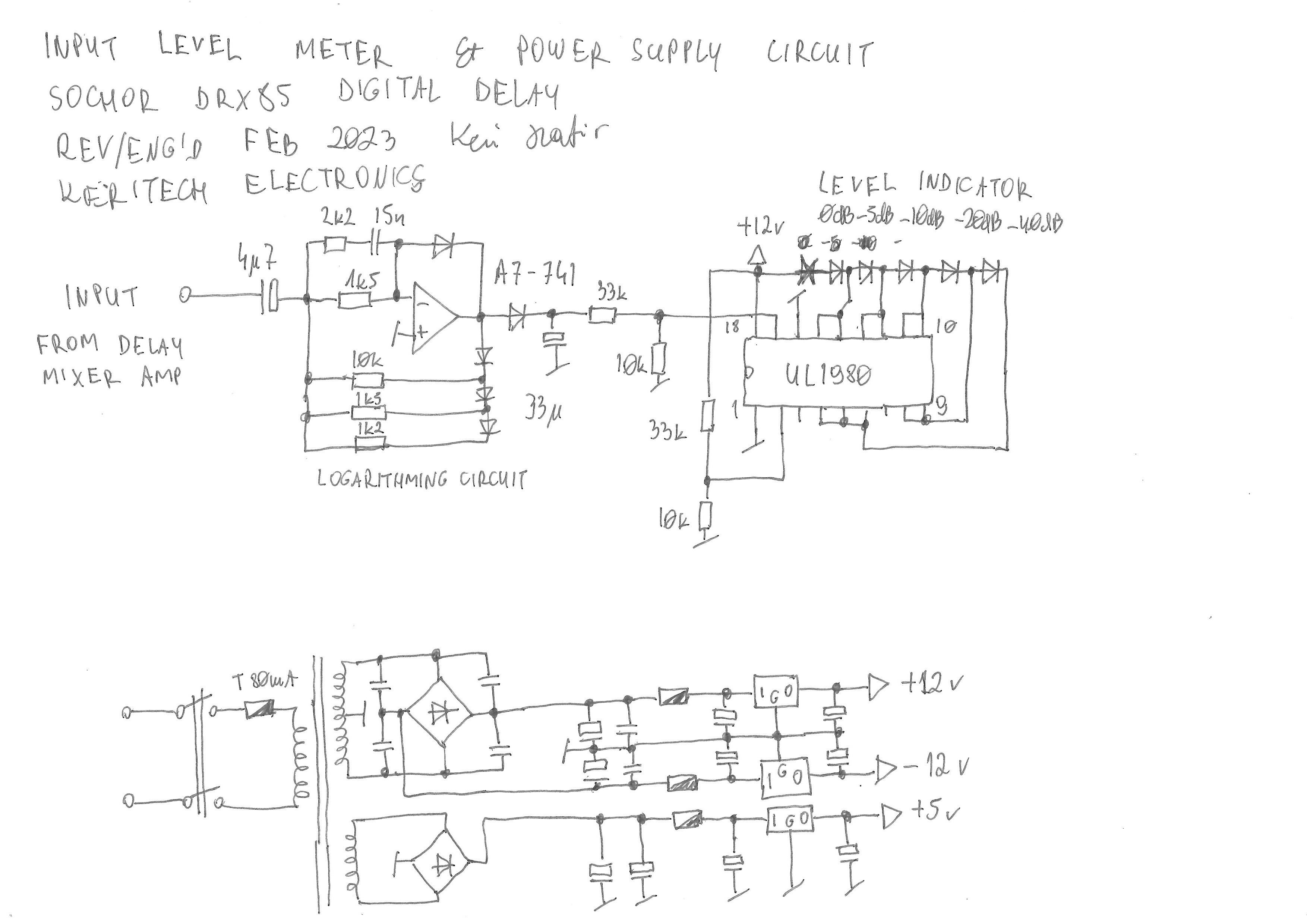
This is just a LED bargraph driver indicating the max signal level which is critical as the ADC is easy to overdrive, very glitchy when it happens. Also, a classic linear regulated PSU with 7812, 7912, discrete diode FULL BRIDGE RECTIFIERs and some flux capacitors... just kidding!
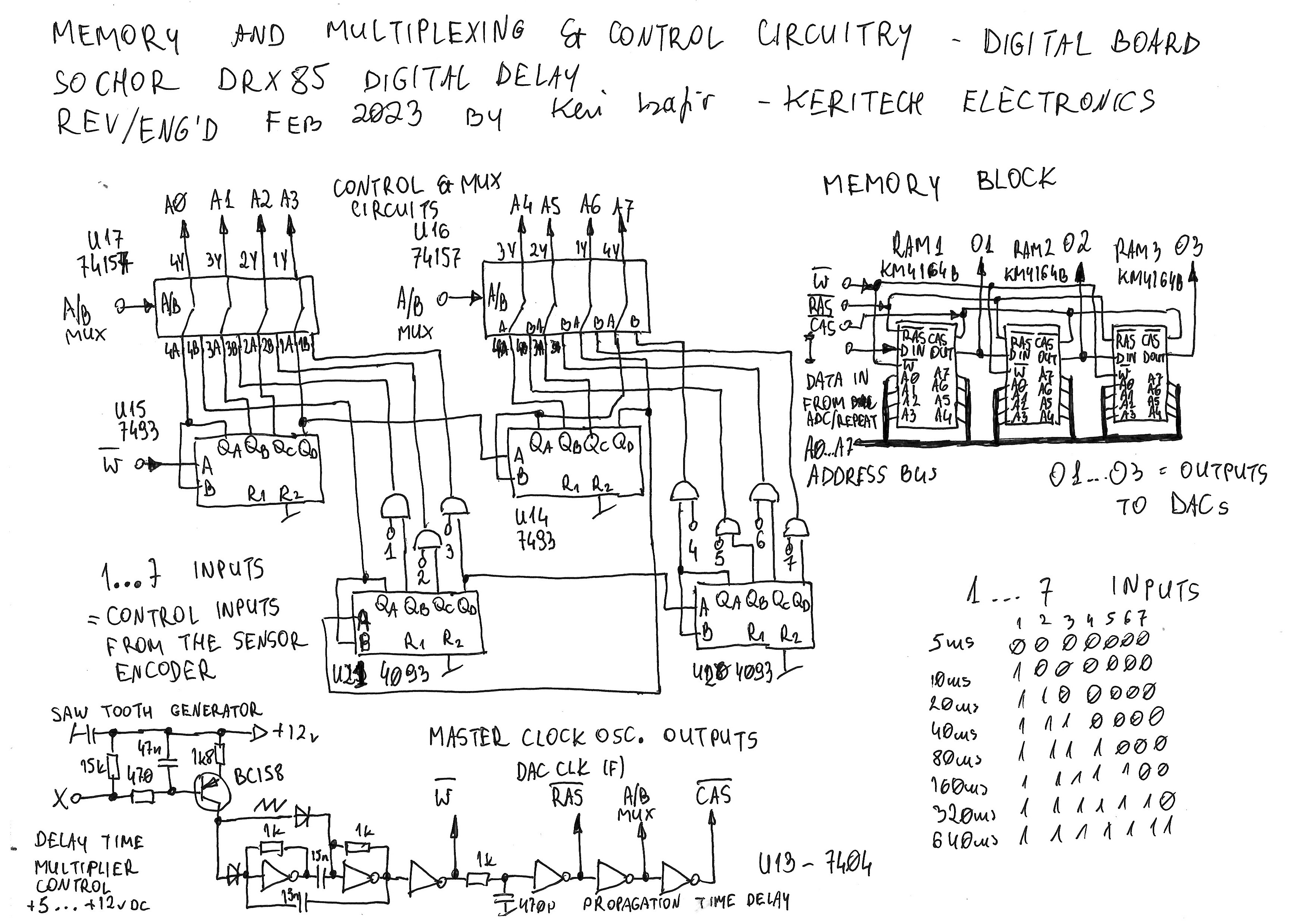
And last but not least, the RAM based delay line. This one kinda eludes me, I'll need to simulate it in Logisim to get a better grip on it... The way I see it, the saw tooth generator and two first inverters form an voltage-controlled oscillator which provides the clock pulses for the whole device, in a sequence: first write enable going up, then ~RAS (row address strobe) going down after one propagation time, A/B multiplexing input going up after double propagation time and then ~CAS (column address strobe) going down after triple propagation time. So, ~CAS will always be tracking ~RAS. By what I read in the KM4164B RAM chip datasheet, the device uses the "lazy write" method so no additional read/write shenanigans here. The 7493 binary counters loop over the addresses of memory cells, some of these addresses will be disabled for shorter delay times thanks to the AND gates which let the counter signal through only when a proper time control line is high. Note the oddity that A7 rather than A4 is selected after A3; these counters work on BCD encoded numbers (0...15, QA being the least significant bit).
Discussions
Become a Hackaday.io Member
Create an account to leave a comment. Already have an account? Log In.