 Just4Fun
This is the first add-on module for the Z80-MBC. It is a 16x GPIOs expansion module based on a MCP23017 IC, and can be easily connected to the Z80-MBC using the IOEXP connector (based on a I2C serial interface), of course on a breadboard...
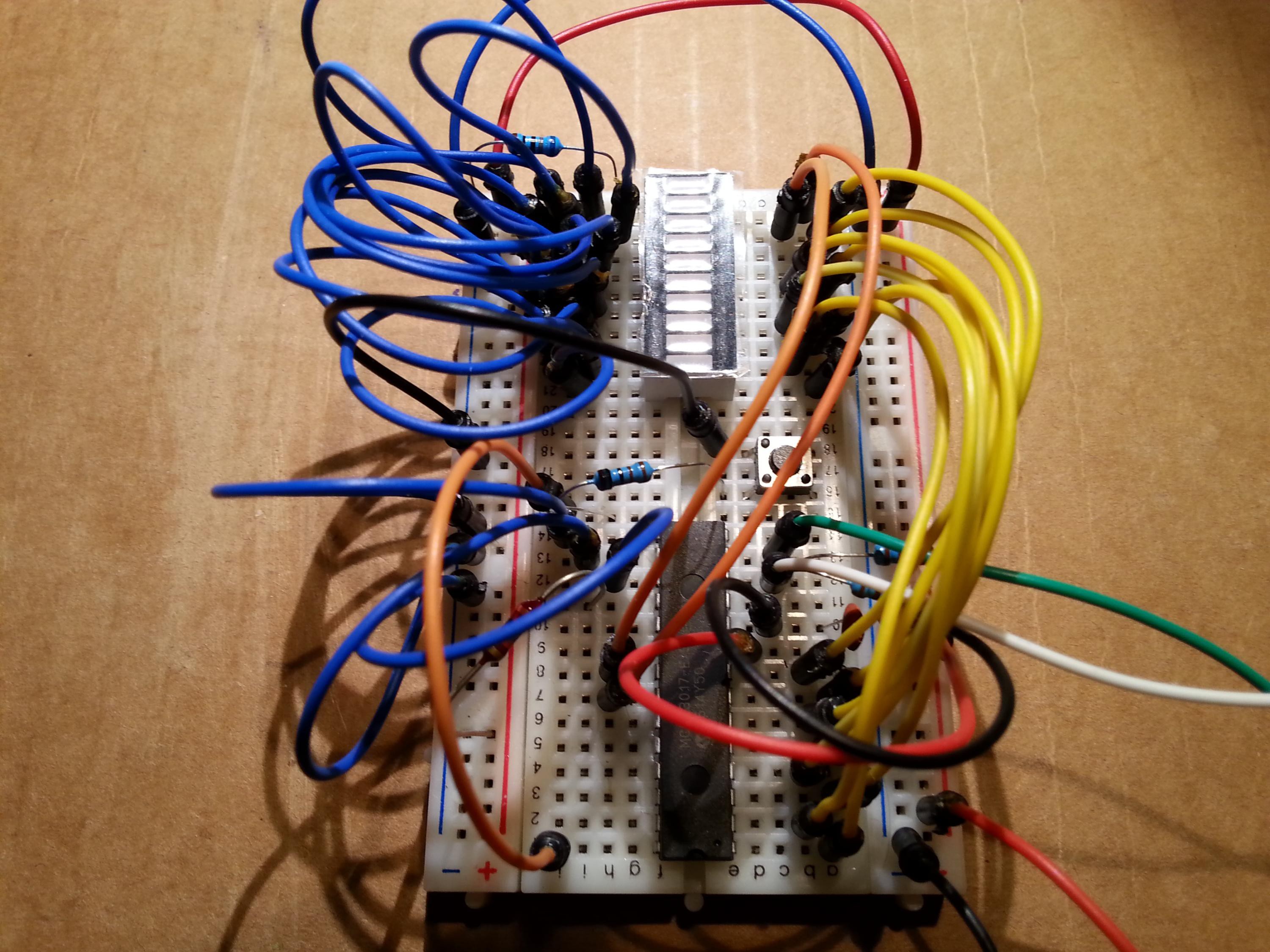
In the Files section I've added the schematic (A080117.pdf) and all the KiCad4 files (A080117 Kicad4.zip).
There is also a new release of the IOS (S221116_R200117_Z80.ino) that takes care of it. During the boot phase, if the GPIO expansion module is found, a specific text is displayed:
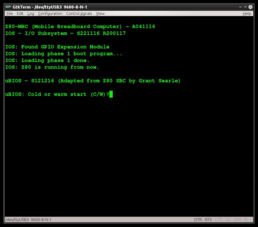
No configuration is needed, just plug it.
Here is a short demo video:
Each GPIO can be configured as input or output, and for each single input it is possible activate a 100K pull-up resistor. Of course this can be done from the Basic language, using new "virtual" I/O addresses as a language extension (if the module is not present, these I/O addresses are simply ignored):
New WRITE I/O addresses:
        0x03:
          // GPIOA write (GPIO Expansion Module):
          //                I/O DATA:    D7 D6 D5 D4 D3 D2 D1 D0
          //                            ---------------------------------------------------------
          //                             D7 D6 D5 D4 D3 D2 D1 D0    GPIOA value (see MCP32017 datasheet)

        0x04:
          // GPIOB write (GPIO Expansion Module):
          //                I/O DATA:    D7 D6 D5 D4 D3 D2 D1 D0
          //                            ---------------------------------------------------------
          //                             D7 D6 D5 D4 D3 D2 D1 D0    GPIOB value (see MCP32017 datasheet)

        0x05:
          // IODIRA write (GPIO Expansion Module):
          //                I/O DATA:    D7 D6 D5 D4 D3 D2 D1 D0
          //                            ---------------------------------------------------------
          //                             D7 D6 D5 D4 D3 D2 D1 D0    IODIRA value (see MCP32017 datasheet)

        0x06:
          // IODIRB write (GPIO Expansion Module):
          //                I/O DATA:    D7 D6 D5 D4 D3 D2 D1 D0
          //                            ---------------------------------------------------------
          //                             D7 D6 D5 D4 D3 D2 D1 D0    IODIRB value (see MCP32017 datasheet)

        0x07:
          // GPPUA write (GPIO Expansion Module):
          //                I/O DATA:    D7 D6 D5 D4 D3 D2 D1 D0
          //                            ---------------------------------------------------------
          //                             D7 D6 D5 D4 D3 D2 D1 D0    GPPUA value (see MCP32017 datasheet)

        0x08:
          // GPPUB write (GPIO Exp. Mod. ):
          //                I/O DATA:    D7 D6 D5 D4 D3 D2 D1 D0
          //                            ---------------------------------------------------------
          //                             D7 D6 D5 D4 D3 D2 D1 D0    GPPUB value (see MCP32017 datasheet)
New READ I/O addresses:
          0x03:
            // GPIOA read (GPIO Expansion Module):
            //                I/O DATA:    D7 D6 D5 D4 D3 D2 D1 D0
            //                            ---------------------------------------------------------
            //                             D7 D6 D5 D4 D3 D2 D1 D0    GPIOA value (see MCP32017 datasheet)
            //
            // NOTE: a value 0x00 is forced if the GPIO Expansion Module is not present

          0x04:
            // GPIOB read (GPIO Expansion Module):
            //                I/O DATA:    D7 D6 D5 D4 D3 D2 D1 D0
            //                            ---------------------------------------------------------
            //                             D7 D6 D5 D4 D3 D2 D1 D0    GPIOB value (see MCP32017 datasheet)
            //
            // NOTE: a value 0x00 is forced if the GPIO Expansion Module is not present
And here is the Basic program used in the video (the HW wiring is shown in the comments):
1 REM * * * GPIO EXPANSION MODULE (A080117) DEMO  * * *
2 REM
3 REM (USER Key -> slow led, GPIO-A(9) Key -> fast led)
4 REM --------------------------------------------------
5 REM Demo HW wiring (see A080117 schematic):
6 REM
7 REM   GPIO-B
8 REM    (J3)
9 REM   +----+   LED
10 REM  | 2  |--->|---+
11 REM  | 3  |--->|---+      RESISTOR
12 REM  | 4  |--->|---+        680
13 REM  | 5  |--->|---+-------/\/\/-----o GND
14 REM  | 6  |--->|---+
15 REM  | 7  |--->|---+
16 REM  | 8  |--->|---+
17 REM  | 9  |--->|---+
18 REM  +----+        |
19 REM                |
20 REM                |
21 REM  GPIO-A        |
22 REM   (J4)         |
23 REM  +----+   LED  |
24 REM  | 2  |--->|---+
25 REM  | 3  |--->|---+
26 REM  | 4  |x
27 REM  | 5  |x
28 REM  | 6  |x
29 REM  | 7  |x     PUSH BUTTON            RESISTOR
30 REM  | 8  |x        ---                   1K
31 REM  | 9  |---------o o------------------/\/\/-----o GND
32 REM  +----+
33 REM
34 REM
35 REM
36 REM --------------------------------------------------
37 REM
38 REM Set MCP23017 GPIOB all pins as output (IODIRB=0x00)
39 OUT 6, 0
40 REM Set MCP23017 GPIOA 0-1 as output, others as input (IODIRA=0xFC)
41 OUT 5, 252
42 REM Set MCP23017 GPIOA 2-7 pull-up resistor on (GPPUA=0xFC)
43 OUT 7, 252
45 REM Left Shift user funcion definition
50 DEF FNLSH(X)=((X*2) AND 255)
55 REM Init GPIO output ports
60 OUT 3, 0 : REM Clear MCP23017 GPIOA port
62 OUT 4, 0 : REM Clear MCP23017 GPIOB port
64 GOSUB 700 : REM Set slow shift
68 REM Main
70 A=1
80 FOR I=0 TO 7
90 OUT 4, A : REM Write to MCP23017 GPIOB port
100 GOSUB 500
110 A=FNLSH(A)
120 NEXT I
130 OUT 4, 0 : REM Clear MCP23017 GPIOB port
135 A=1
140 FOR I=0 TO 1
150 OUT 3, A : REM Write to MCP23017 GPIOA port
160 GOSUB 500
170 A=FNLSH(A)
190 NEXT I
200 OUT 3, 0 : REM Clear MCP23017 GPIOA port
210 GOTO 70 : REM Play it again, Sam...
220 REM
500 REM * * * * * DELAY SUB
505 FOR J=0 TO K
507 IF INP(0)=1 THEN GOSUB 700 : REM Read USER key
508 IF (INP(3) AND 128)=0 THEN GOSUB 600 : REM Read MCP23017 GPIOA 7 key
510 NEXT J
520 RETURN
530 REM
600 REM * * * * * SET FAST SHIFT SUB
610 K=1
620 OUT 0, 1 : REM USER led ON
630 RETURN
640 REM
700 REM * * * * * SET SLOW SHIFT SUB
710 K=30
720 OUT 0, 0 : REM USER led OFF
730 RETURN
--> Important Note: If you use a terminal emulator to send the file to the Z80-MBC, configure it to add a 40ms delay each "end of line". Because Arduino bootloader "environment" doesn't manage any handshaking on the serial port, this is needed for a correct file transfer.
Discussions
Become a Hackaday.io Member
Create an account to leave a comment. Already have an account? Log In.
Very nice ASCII schematic :)
Are you sure? yes | no
:-)
Are you sure? yes | no