 Bharbour
Before I get started on the details of this clock, I would like to give a big Thanks to the people at OSH Park. I have been using their services for about 9 years now, and they provide consistently good quality boards at a reasonable price. If you look through my projects here, all the PCBs I have designed are purple. Their service makes it possible for me to build multiple projects in a year, compared to the old days where a run of PCBs was so expensive that 1 or 2 a year was all that was affordable. Thanks, OSH Park!
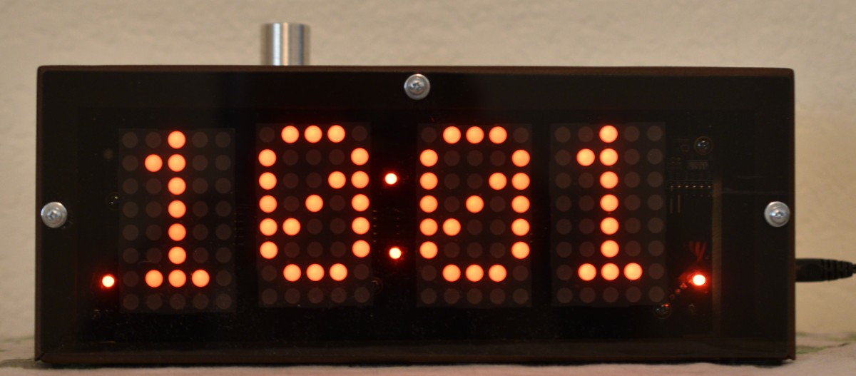
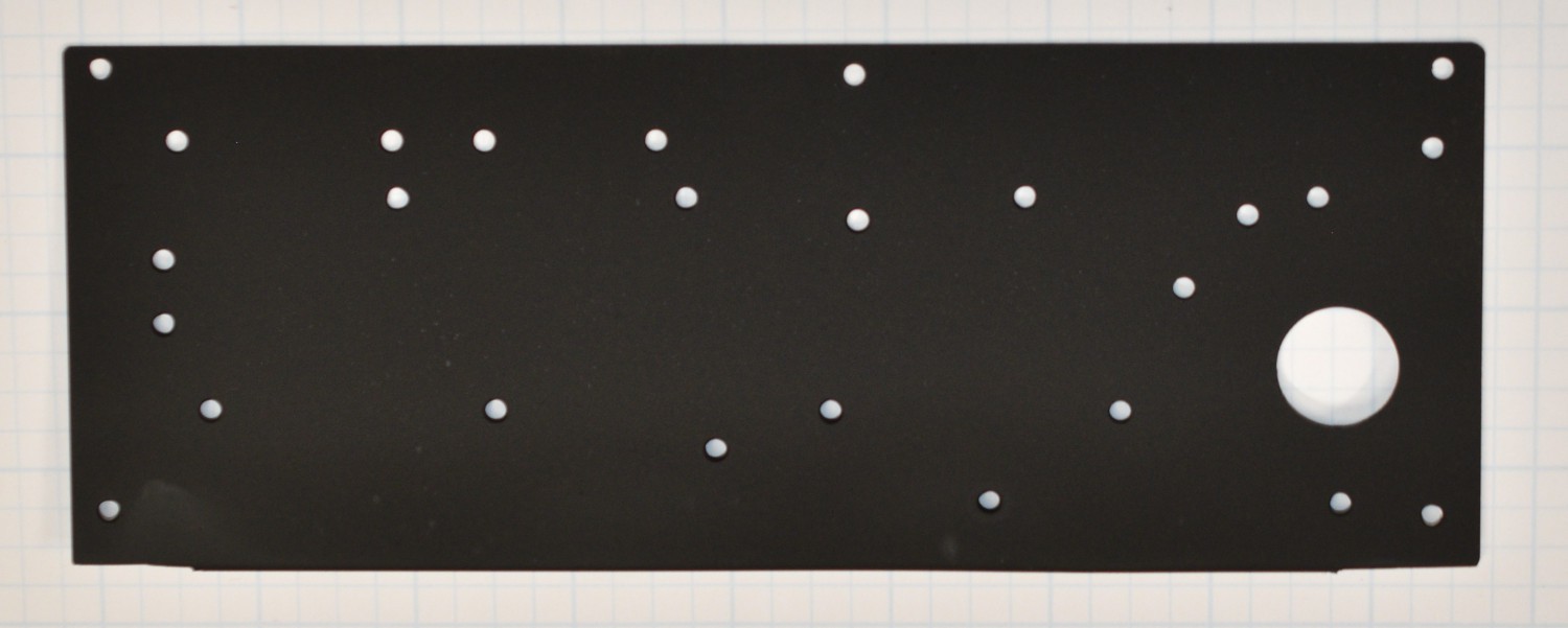
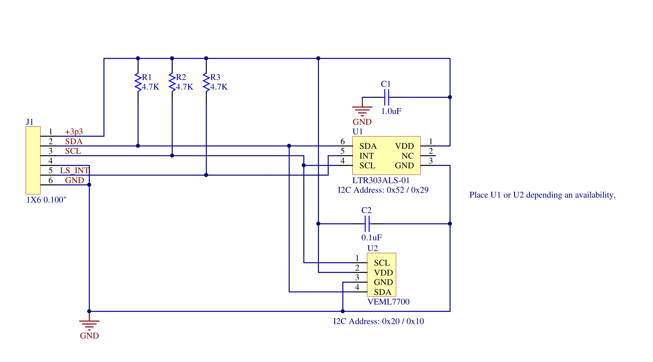
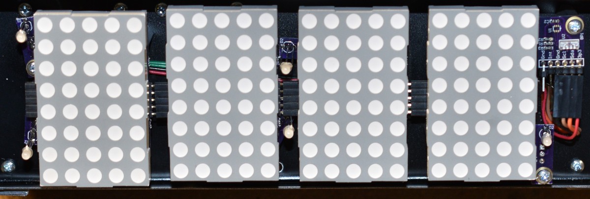
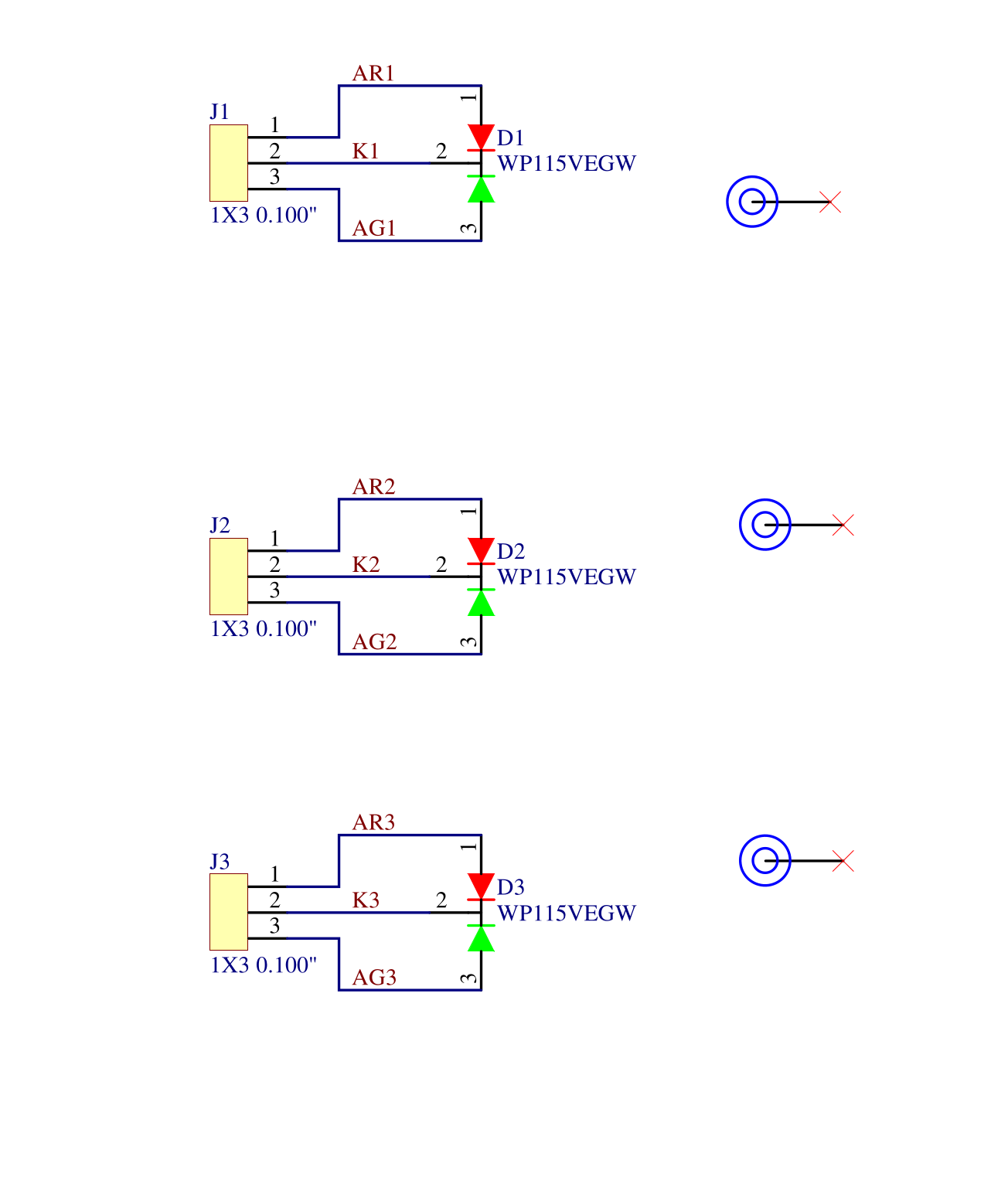
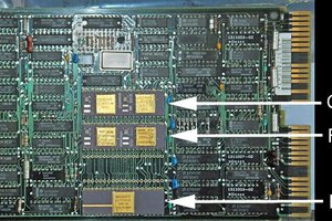
Most of the boards in this project are mounted with threaded standoffs to a single plate that attaches to the outer skin of the case. The front side of that plate has the 4 display driver PCBs, small LED mounting boards for the discrete red/green indicator LEDs and an ambient light sensor board. The LED character displays and the discrete LED indicators are all capable of displaying in red or green, under control of the display driver chips.
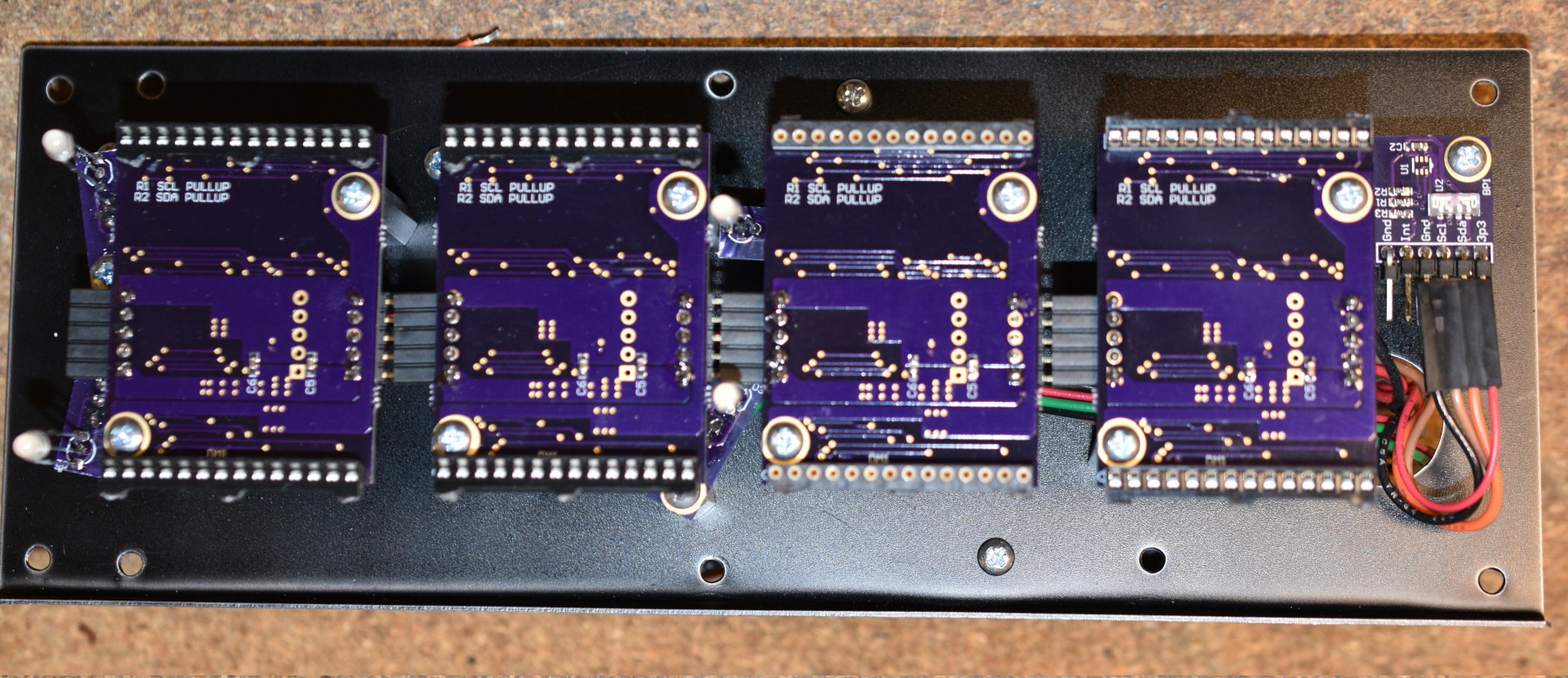
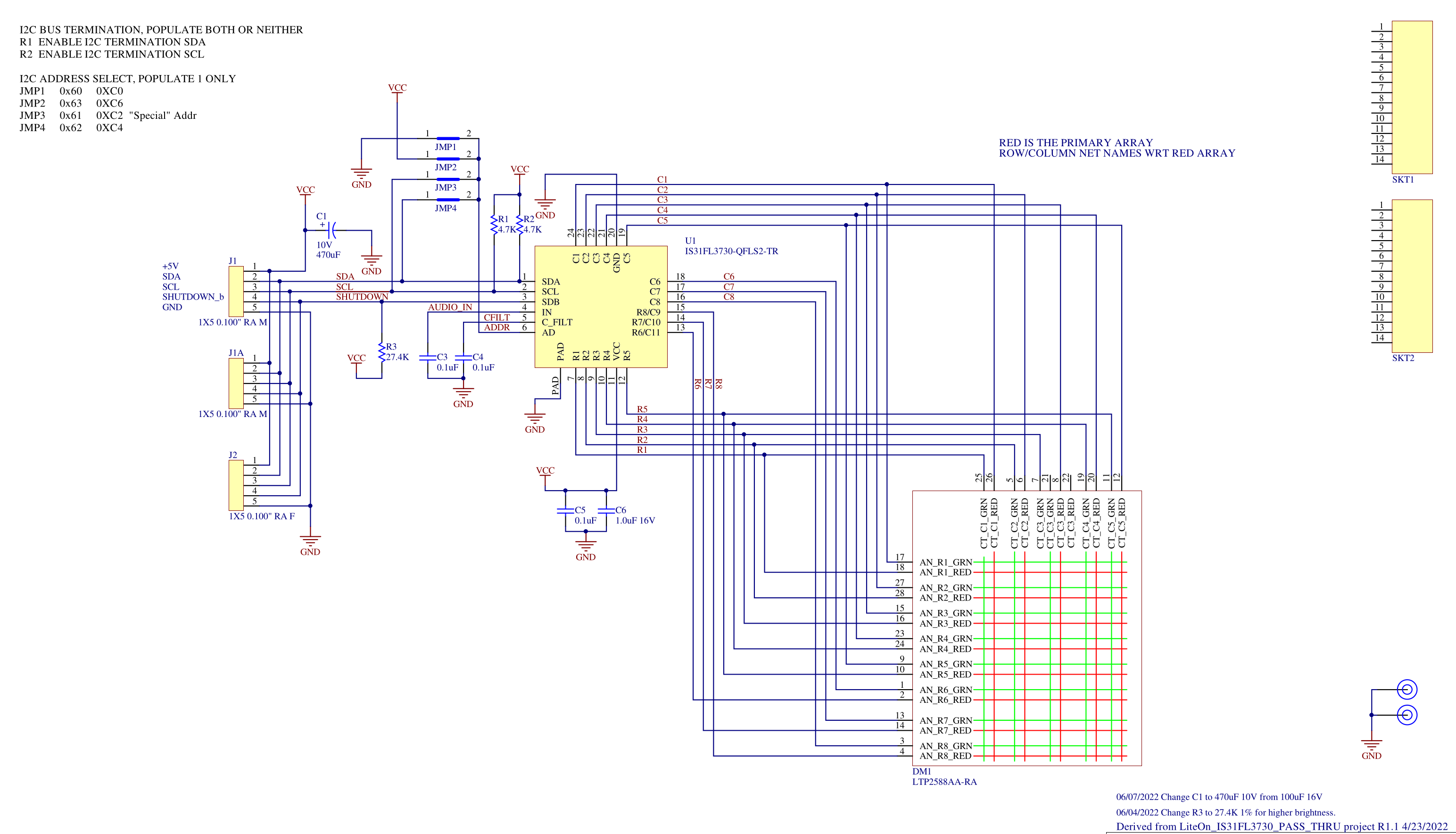
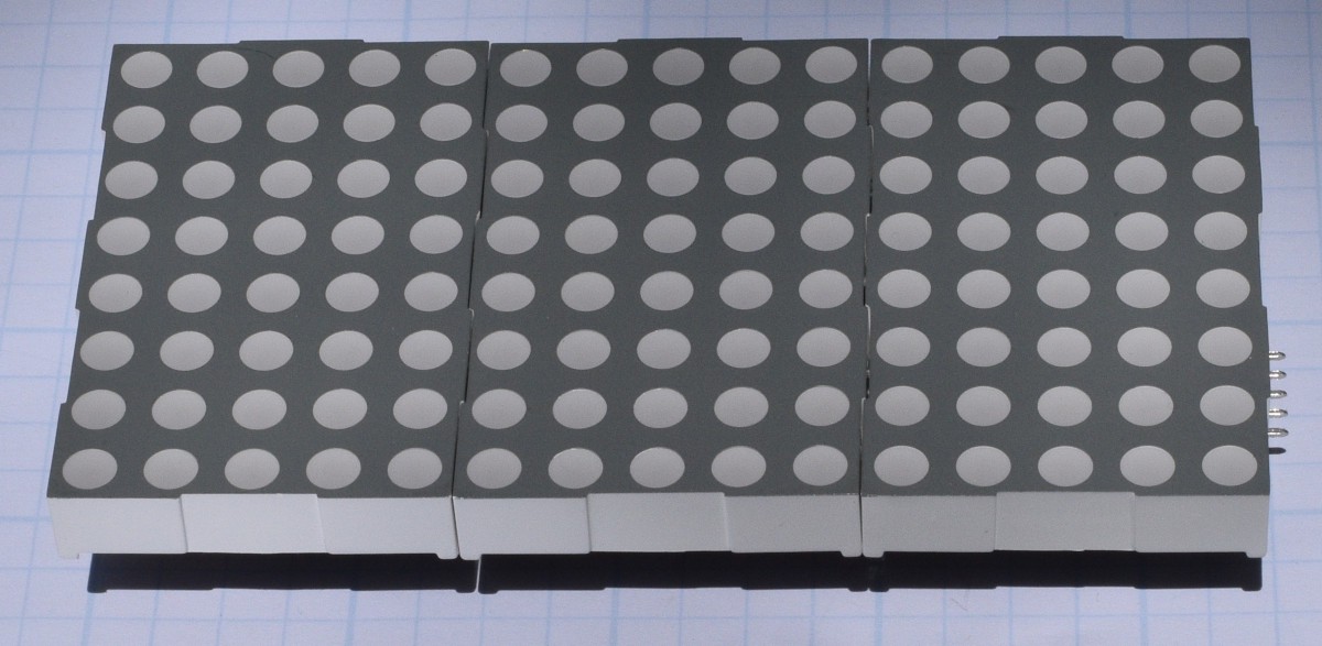
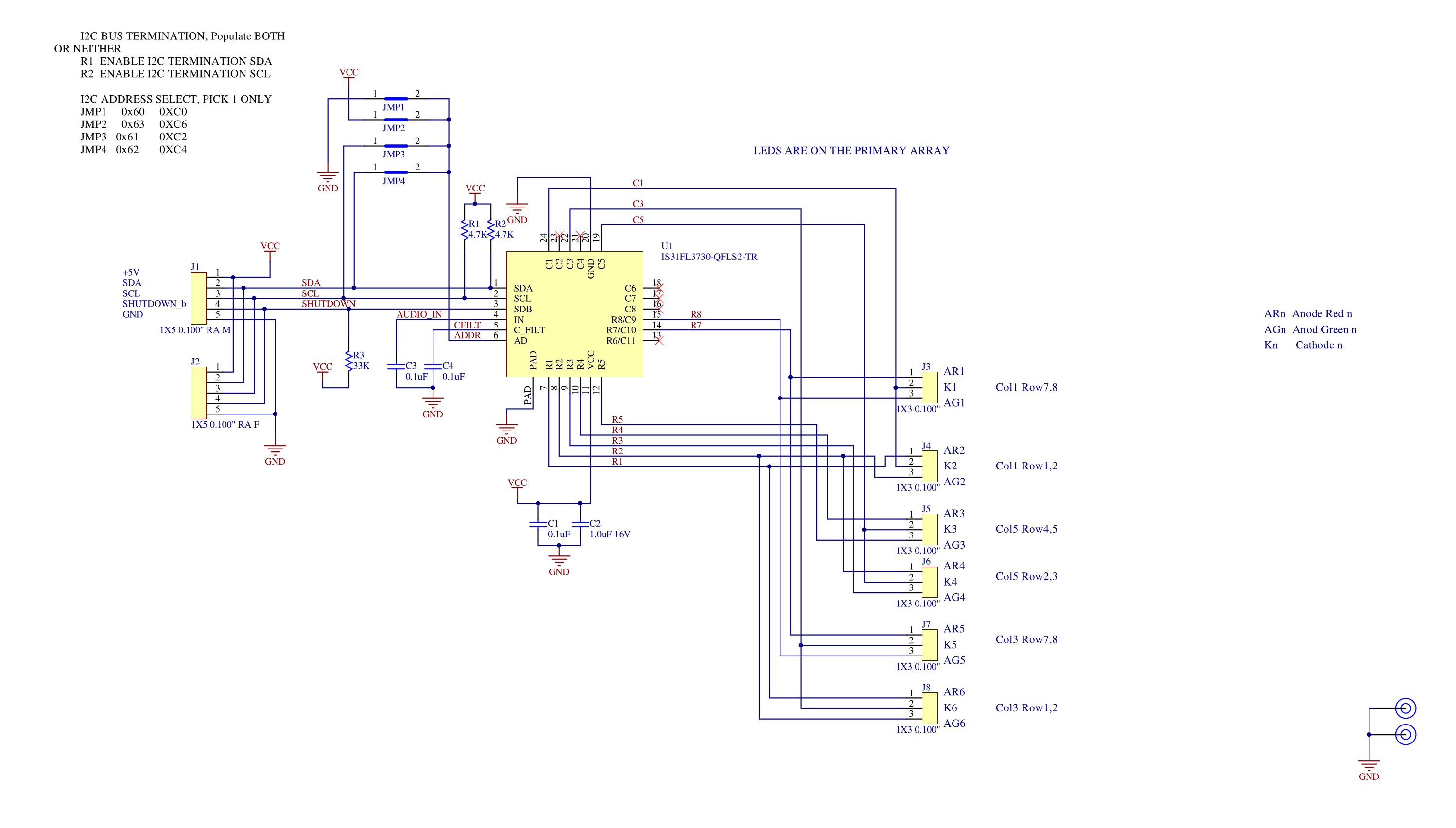
The display drive boards have "stacking" connectors to interconnect up to 4 characters in a row, passing power and I2C signals directly from board to board. The limit of 4 characters comes from the number of choices for the I2C address offered by the IS31FL3730 driver chips. The driver boards can be assembled to be in contact with the characters on either side, or to have the inter-character space be empty. In this case, the inter-character spaces are empty with the exception of the 2 discrete LEDs between the hours and minutes displays. At the left end of the display are two discrete LEDs to indicate AM/PM when run in 12 hour mode. At the right end is the ambient light sensor which is used to dim the displays according to the room lighting. After this picture was taken, another discrete LED was added in the lower right corner to indicate whether the alarm is set.
In previous projects with these displays, I left the inside of the display area bare metal, and it reflected enough light that too much of the internals are visible. Painting the mounting plate black was done to try to reduce that.
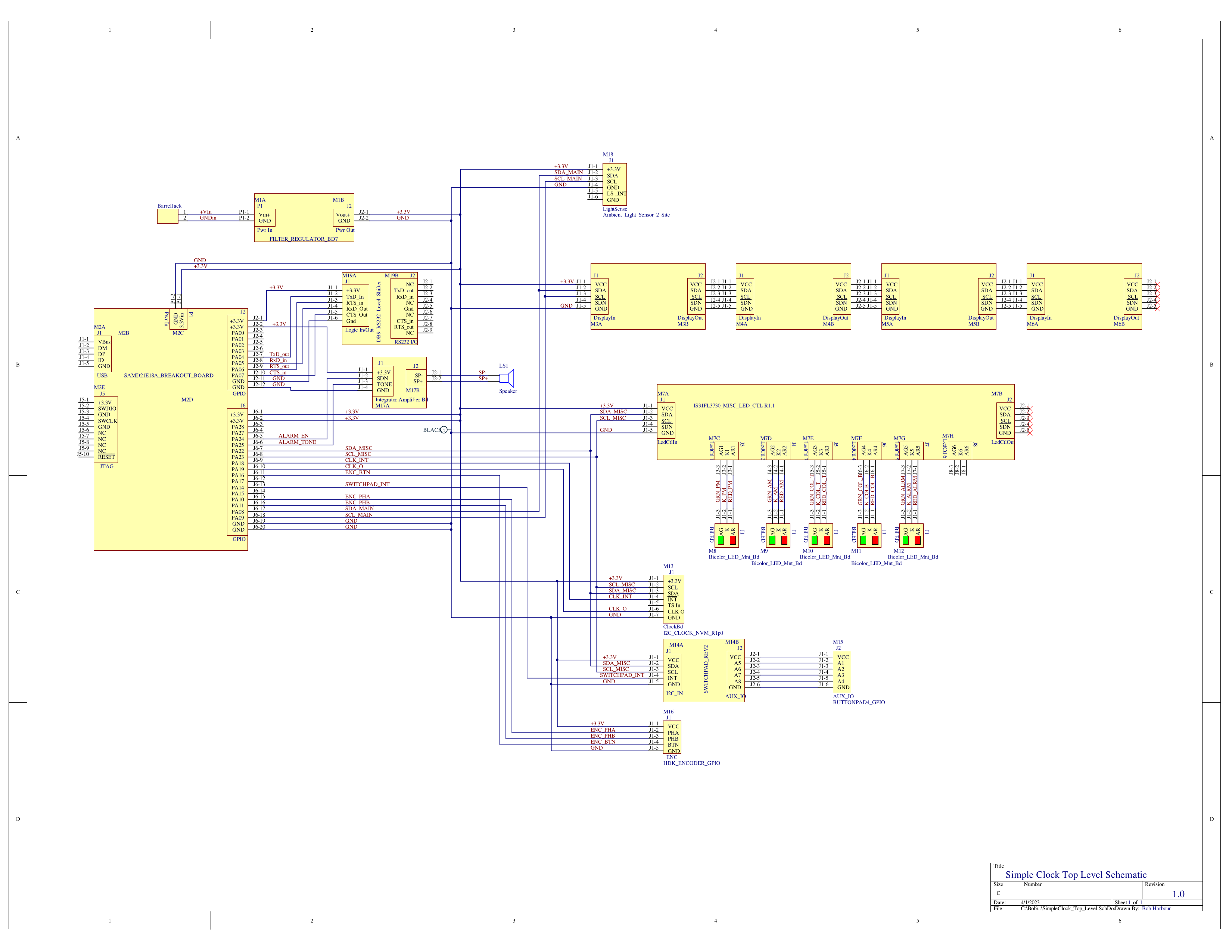
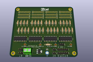
On the back side of the mounting plate (L to R), the Filter Regulator board, Miscellaneous LED Controller board, Clock board and the CPU board can be seen.
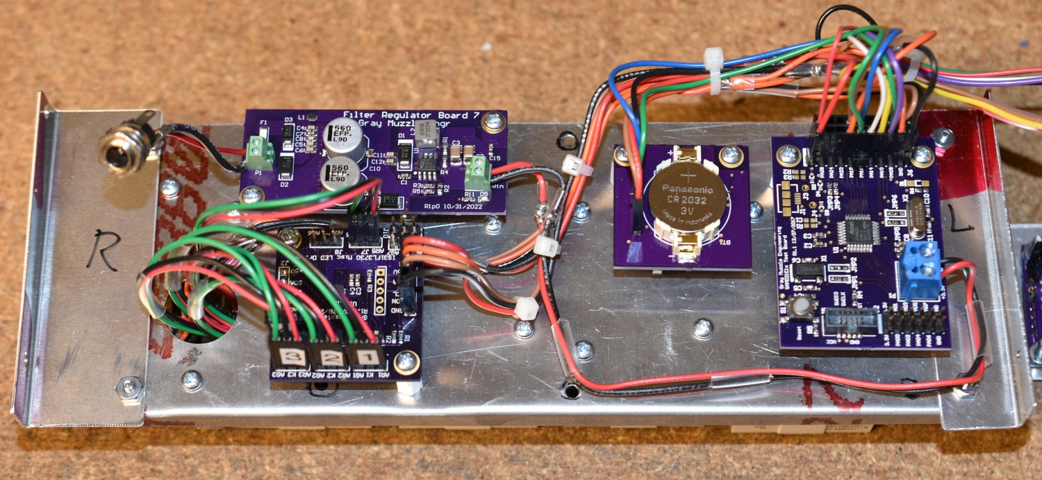
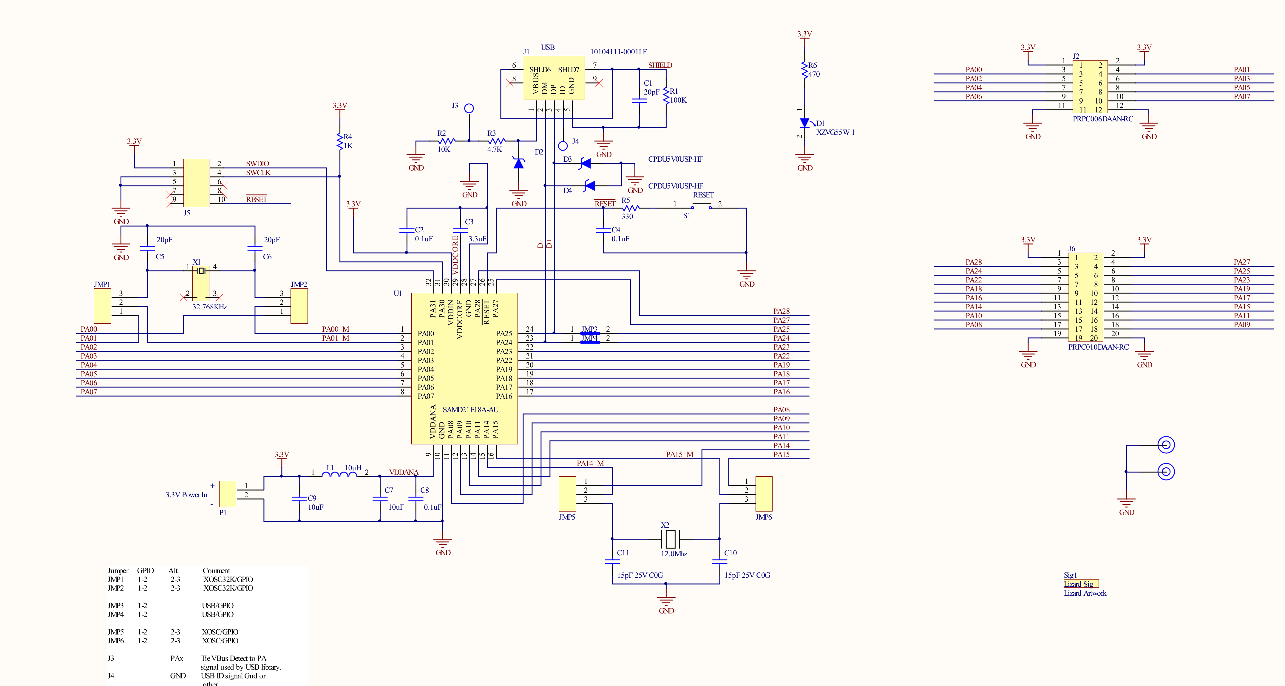
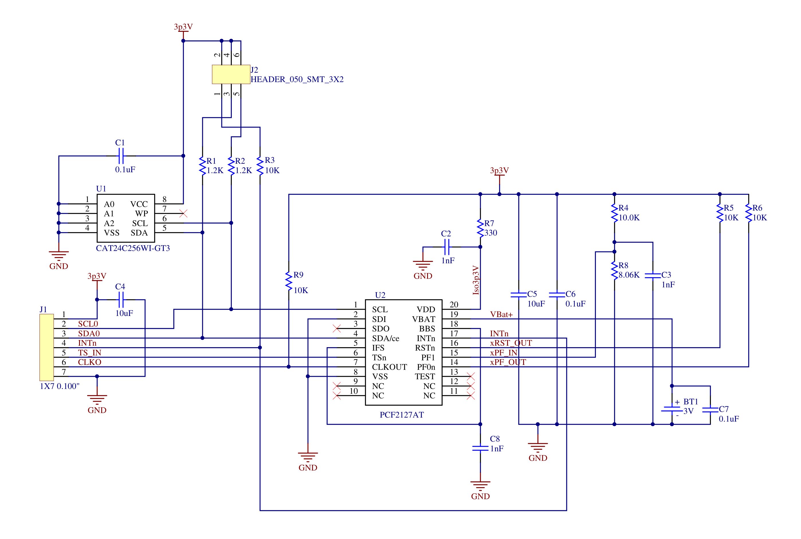
Input power comes into the system at 12V on the upper left corner of the picture. It is regulated down to 3.3V for the rest of the system on the Filter Regulator board. The board below the Filter Regulator board is the Miscellaneous LED Control board which handles all of the discrete LEDs on the front side of the plate. To the right of these boards is the clock board. It is an NXP PCF2127 clock/calendar chip with a backup battery mounted on the exposed side of the board for easy access. The rightmost board is the Processor board. It uses an ATSAMD21E18A chip.
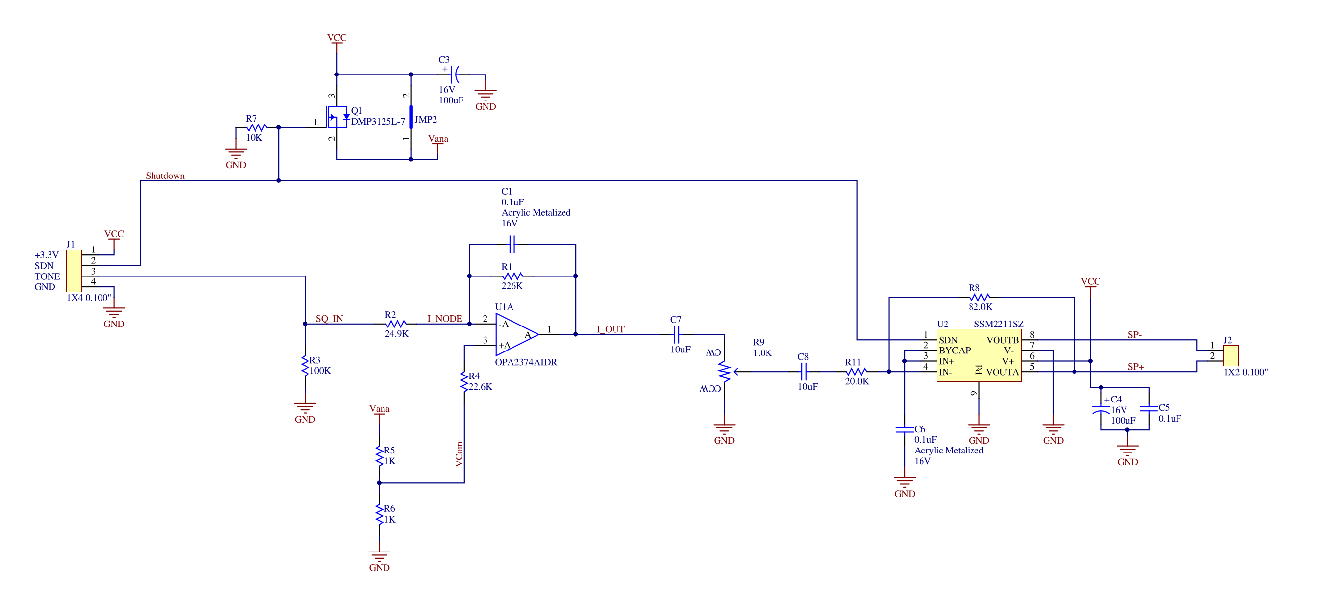
Almost all of the communications in this clock are done via I2C. The only part of this clock that is not interfaced via I2C is the rotary encoder. Two I2C ports are configured on the processor. The Miscellaneous LED Controller board uses an IS31FL3730 chip (same as the character driver boards), which must go on a different bus than the 4 character display driver boards because there would be an address collision. The ambient light sensor lives on the same I2C bus as the character displays. The Clock and part of the user interface live on the same I2C bus as the Miscellaneous LED Controller.
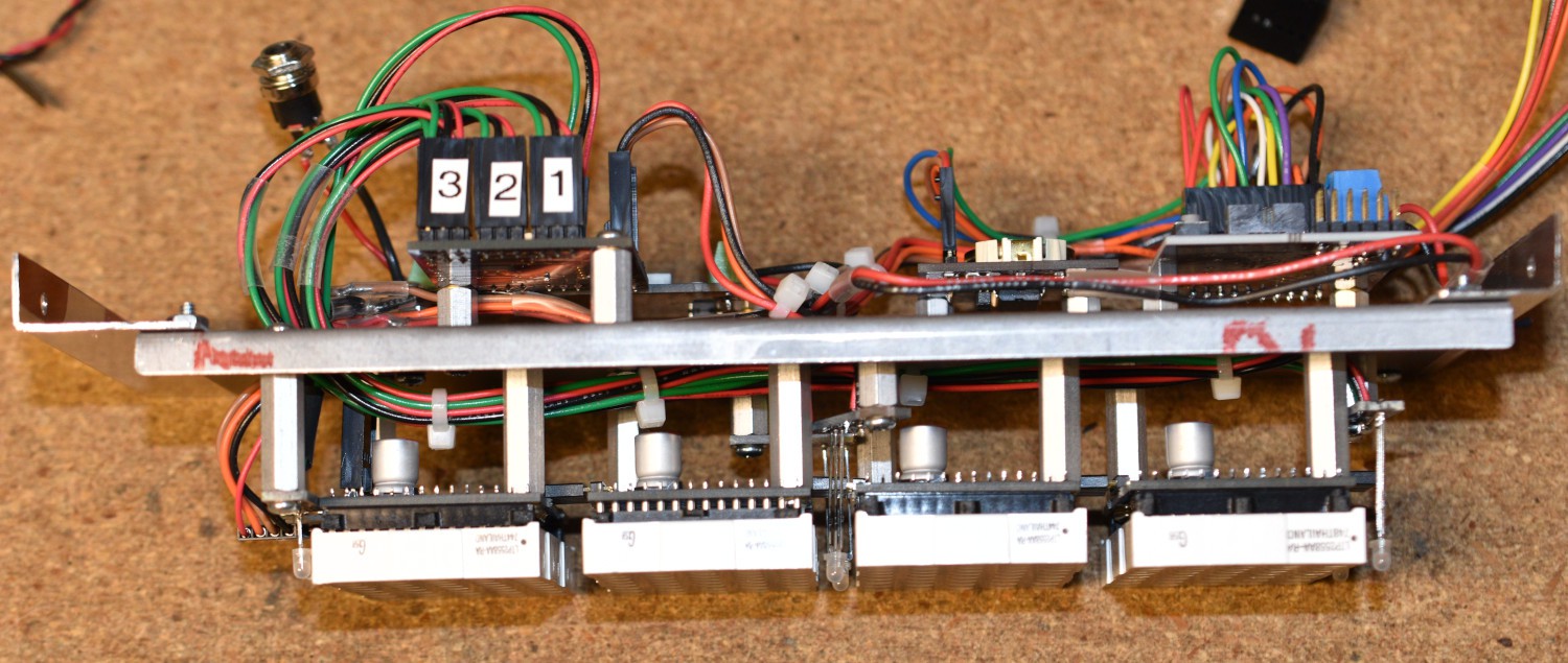
Both sides of the electronics plate can be seen here. The display modules have been installed on the character driver boards too.
One of the ways to minimize traffic on the I2C buses in a system like this is to use the "Interrupt" signal from various I2C interfaced devices. The clock chip is configured in software to drive an interrupt signal once per second, so it is not necessary to poll the clock continuously, just wait for a rising edge on the interrupt signal which is tied to a GPIO input. Similarly, the user interface uses an I2C port expander chip...
Read more »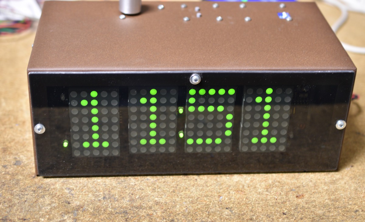


 cselzey
 Ken Yap
I like up/down better than fast/slow with separated hours and minutes for buttons. A couple of other projects that I have done used this and it works pretty well.
Try it and see