 zpekic
Context
Given that this CPU implementation is an almost canonical example of microcoded design as envisioned by AMD - and a showcase of their Am29XX and Am25XX ICs - it is very helpful to go over at least chapters I and II of the "Bit-slice microprocessor design" book for better understanding. After that, the application note provides a great explanation of this specific CPU implementation. All source files to implement the CPU are under this folder.
(for execution unit, which the other major part of the CPU, see this log)
Control unit
(for good discussion of these refer to "Bit-Slice Design: Controllers and ALUs" by D. E. White)
The key to micro-coded CPUs/controllers is their control unit. Typically this control unit has a very limited set of instructions it can recognize:
- has a program counter ("micro-program counter" == uPC)
- uPC can be modified in a very simple way: increment, hold the same, jump, jump to an externally provided address
- sometimes subroutine calls and returns are supported (to a limited level, 2-4)
This is how the control unit for Am9080 looks like:
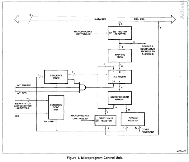
Let's identify and describe each element as defined in the code:
- Instruction register
8-bit register with input connected to the D-bus (instructions come always from there, either through memory read, or presented by external hardware as a result to INTA (interrupt acknowledge cycle)
    -- instruction register ---
    u1516: am25ls377 port map (
        clk => CLK,
        nE => pl_instregenable,
        d => DBUS,
        q => current_instruction
    );
current_instruction is the 8-bit opcode of the currently executing machine instruction. Where is the nE (load enable) signal coming from? From microcode instruction which is executed during instruction fetch:
;0004 FETCH: ALU DOUBLE,PC,PC,FTOB.F & OR & ZA & ALUC & BASW & /IOC IN,,TO.A & MEMR & IF ,INV,READY & NUM, $
0004 0100000000010000 0010010111010001 0011011111111110 11011100;
;
;0005 INCPC & IF D.R. ,HOLD & NUM,HLDD & NOC
0005 1100000000110000 1110100111110001 0011011111111110 11000100;
in other words, signal pl_instregenable is microinstruction bit 55 (MSB) and this is the only time when it appears low.
- mapping PROM
as explained here, this memory is a "many to one" lookup table.
    -- u11, u12, u13 ----------
    mapper_rom: rom256x12 Port map (
        address => current_instruction,
       data => instruction_startaddress(11 downto 0)
   );
For each op-code presented as 8-bit address (current_instruction) a 12-bit data will appear on the output (only 9-bits are of interest as the microprogram memory is 512 words deep). The instruction_startaddress is then presented as one input of the Am2909-12 device:
- Sequencer
In original schema these are 3 4-bit Am2909 devices, merged here together:
    -- to save some FPGA area, 3 * 2909 = 1 * 2909-12
    u21u22u23: am2909x12 port map (
        S => sequence(1 downto 0),
        R => u_immediate,
        D => instruction_startaddress,
        ORi => interrupt_or_mask,
        nFE => sequence(3),
        PUP => sequence(2),
        nRE => '0',
        nZERO => nRESET,
        nOE => '0',
        CN => '1',
        CLK => CLK,
        -- Output ports
        Y    => ma,
        C4    => open
    );
Looking inside the Am2909-12, we see that the 12-bit uPC inside the Am2902-12 will be loaded when sequence(3 downto 0) == "1011"
The sequence is coming from another simple lookup table:
   --- sequencer rom ----
    u14: rom32x8 port map ( -- TODO: it is actually 16*5 only
        nCS => '0',
        address(3 downto 1) => pl_nextinstrselect,
        address(0) => u8474_u8475_pin15,
        data(4 downto 0) => sequence
    );
This sequence is marked "D" and the address input must be 0010 (2) to return it:
type rom is array(0 to 15) of std_logic_vector(4 downto 0);
constant lookup: rom := (
            "01000", -- C
            "01001", -- R
            "01011", -- D
            "01001", -- R
            "01000", -- C
            "00101", -- SBR
            "01001", -- R
            "00010", -- RTN
            "11010", -- F
            "00101", -- SBR
            "00000", -- POP
            "00001", -- PR
            "01001", -- R
            "00100", -- PUSH
            "01001", -- R
            "11010"  -- F
                );
However we see that the microinstruction word only defines upper 3 bits of this lookup address, the lowest address bit of the lookup table is actually the result of the condition check (u8474_u8475_pin15 is output of a 16-to-1 MUX). This means that the sequencer instruction are "paired" - XXX0 defines what Am2909-12 should execute when condition fails and XXX1 when condition passes. For example:
if (condition) then C else R //continue else load from R reg)
if (condition) then D else R //load from D else load from R reg)
if (condition) then C else SBR //continue else jump to subroutine
etc...
Searching for D/R combination in microcode, we find it only in instructions 005 and 00C:
;0004 FETCH: ALU DOUBLE,PC,PC,FTOB.F & OR & ZA & ALUC & BASW & /IOC IN,,TO.A & MEMR & IF ,INV,READY & NUM, $
0004 0100000000010000 0010010111010001 0011011111111110 11011100;
;
;0005 INCPC & IF D.R. ,HOLD & NUM,HLDD & NOC
0005 1100000000110000 1110100111110001 0011011111111110 11000100;
;
;0000
;0000 ;HOLD AND MEMORY REFERENCE SUBROUTINES AND HANDLERS:
;0000
;
;0000 ORG 10
;
;000A HLDSB: NALU & IOC & HLDA & IF R.RTN, INV, HOLD & NUM, $
000A 1100000000101001 1010100111111000 0011010101010100 01XXXXXX
;
;000B HLDF: NALU & IOC & HLDA & IF R.F, INV,HOLD & NUM, $
000B 1100000000101111 1010100111111000 0011010101010100 01XXXXXX
;
;000C HLDD: NALU & IOC & HLDA & IF D.R,,HOLD & NUM, $
000C 1100000000110000 1110100111111000 0011010101010100 01XXXXXX
Highlighed are bit 41, 40, 39 because this 3 bit field is the pl_nextinstrselect:
--    39-41    3             Next Instruction Select
alias pl_nextinstrselect: std_logic_vector(2 downto 0) is pl(41 downto 39);
As expected, start address of the instruction is loaded into uPC right after fetch, and in the same cycle PC is incremented.
- microprogram memory
with size of 512*56, it is clear that the address will be lower 9 bits coming from Am2909-12 sequencer output, and the data will be the 56-bits that drive every other signal in the design
   --- microcode rom ---
   microcode_rom: rom512x56 Port map (
        address => ma(8 downto 0),
        data => u
  );
The 56-bit word is split into "fields" of various sizes. Unlike some more complex microcode architectures which have variable meaning fields of differing sizes, here every microinstruction has the same fields:
signal u: std_logic_vector(55 downto 0);        -- microcode output
signal pl: std_logic_vector(55 downto 0);        -- microcode register
---------------------------------------
--    Bits    Length    Description I
---------------------------------------
--    0-2    3             ALU Source (I0-I2 of the Am2901A's)
alias pl_alu_source: std_logic_vector(2 downto 0) is pl(2 downto 0);
--    3-5    3             ALU Function (I3-I5 of the Am2901A's)
alias pl_alu_function: std_logic_vector(2 downto 0) is pl(5 downto 3);
--    6-8    3             ALU Destination (I6-I8 of the Am2901A's)
alias pl_alu_destination: std_logic_vector(2 downto 0) is pl(8 downto 6);
--    9-12    4             ALU "B" Address
alias pl_alu_b: std_logic_vector(3 downto 0) is pl(12 downto 9);
--    13-16    4             ALU "A" Address
alias pl_alu_a: std_logic_vector(3 downto 0) is pl(16 downto 13);
--    17        1             Single/Double Byte
alias pl_not8or16: std_logic is pl(17);
--    18        1             Cn for least significant Am2901A slice
alias pl_carryin: std_logic is pl(18);
--    19        1             Rotate and Swap Control (formatted)
alias pl_rotateorswap: std_logic is pl(19);
--    20-21    2             Update/keep flags
alias pl_updateorkeepflags: std_logic_vector(1 downto 0) is pl(21 downto 20);
--    22        1             "A" Address Switch
alias pl_aswitch: std_logic is pl(22);
--    23-24    2             Am2901A Output Steering Control
alias pl_outputsteer: std_logic_vector(1 downto 0) is pl(24 downto 23);
--    25-26    2             Data Bus Enable Control
alias pl_databusenable: std_logic_vector(1 downto 0) is pl(26 downto 25);
--    27-32    6             HLDA, MEMW, MEMR, I/OW, I/OR, INTA (Am9080A System Control Outputs)
alias pl_syscontrol: std_logic_vector(5 downto 0) is pl(32 downto 27);
--    33        1             "B" Address Switch
alias pl_bswitch: std_logic is pl(33);
--    34-37    4             Condition Code Select
alias u_condcode: std_logic_vector(3 downto 0) is u(37 downto 34);
--    38        1             Condition Code Polarity Control
alias u_condpolarity: std_logic is u(38);
--    39-41    3             Next Instruction Select
alias pl_nextinstrselect: std_logic_vector(2 downto 0) is pl(41 downto 39);
--    42-53    12         Numerical Field
alias u_immediate: std_logic_vector(11 downto 0) is u(53 downto 42);
--    54        1             Numerical Field to Data Bus Control
alias pl_immediatedatabus: std_logic is pl(54);
--    55        1             Instruction Register Clock Enable
alias pl_instregenable: std_logic is pl(55);
-----------------------------------------
To note:
- Control unit is driven by fields in the microinstruction too - bits 34 to 53 are "looped back" to control execution. Essentially this is defining a "if (condition) then / else" statements. For this to work, u_condcode, u_polarity, pl_nextinstrselect, u_immediate fields are needed. u_immediate is a 12-bit data field which allows "GOTO xxx" or "GOSUB xxx" by providing the target microinstruction address xxx.
- Control signals that come out from microprogram memory are consumed:
- directly, as "u_xxx" signals - this means that they are available in the same cycle (with delay) as the microinstruction that is executing
- indirectly, through the "pipeline" register (pl_xxx signals) - this register is 44 bits long and is holding the control signals stable while the controller is deciding on which next microinstruction to execute.
Some pipeline pl_xxx signals are directly connected to CPU control pins:
   u7172: Am25LS374 port map (
              clk => CLK,
           nOE => pl(27),
           d(0) => '0', -- ignored
           d(1) => '0', -- ignored
           d(2) => u83_pin6,
           d(3) => u(32),
           d(4) => u(31),
           d(5) => u(30),
           d(6) => u(29),
           d(7) => u(28),
           y(0) => open,
           y(1) => open,
           y(2) => WAITOUT,
           y(3) => pl(32), --nINTA,
           y(4) => pl(31), --nIOR,
           y(5) => pl(30), --nIOW,
           y(6) => pl(29), --nMEMR,
           y(7) => pl(28)  --nMEMW
            );
    HLDA <= not pl(27);
    nINTA <= pl(32);
   nIOR <= pl(31);
   nIOW <= pl(30);
   nMEMR <= pl(29);
   nMEMW <= pl(28);
Discussions
Become a Hackaday.io Member
Create an account to leave a comment. Already have an account? Log In.