 zpekic
Context
Given that this CPU implementation is an almost canonical example of microcoded design as envisioned by AMD - and a showcase of their Am29XX and Am25XX ICs - it is very helpful to go over at least chapters I and II of the "Bit-slice microprocessor design" book for better understanding. After that, the application note provides a great explanation of this specific CPU implementation. All source files to implement the CPU are under this folder.
(for control unit, which the other major part of the CPU, see this log)
Execution unit
This part of the CPU is where registers (both program accessible AF, BC, DE, HL, PC, SP) and temporary / internal are held, and modified by passing through ALU and other data paths.
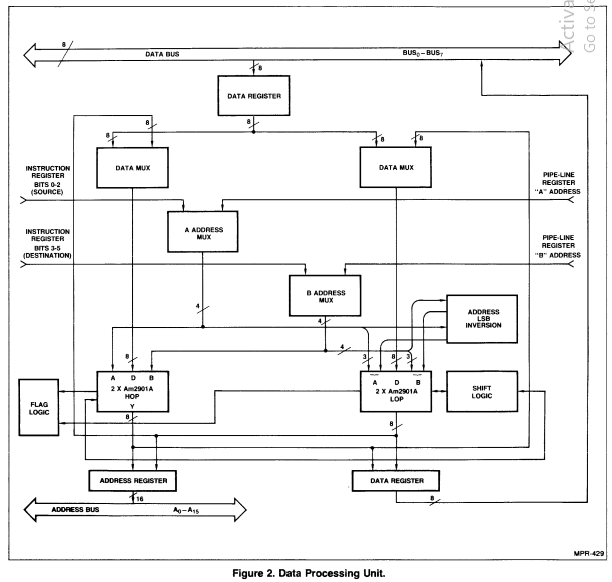
The central component of the execution unit is a set of 4 Am2901 bit-slices. This fascinating chip was the de-facto standard during the heyday of the era (1970ies), although Intel, MMI, and Texas Instruments had bit-slices too.
The most important question when designing with bit-slices is how to map the design registers (program accessible and internal only) to the available set of slice registers. Intel 8080 (and 8085) has 6 16-bit program accessible registers so they can be mapped in different ways, for example:
| Mapping --------- (registers 0..15) | Number of slices | Pros | Cons |
| By 8-bit register ---------- B C D E H L M A SP.H SP.L PC.H PC.L ? ? ? ? | 2 | Cost savings! (only 2 slices), fast for 8-bit operations, max register utilization | Slow for 16-bit operations, additional external 16-bit register needed |
| By 16-bit register pair ---------- BC DE HL MA SP PC ?? ?? ?? ?? ?? ?? ?? ?? ?? ?? | 4 | Fast for 16-bit operations, simpler design | 4 slices needed, additional external MUXs and other logic for 8-bit operations, slower for 8-bit operations, many unused registers (could be viable for Z80) |
| Mixed --------- BC CB DE ED HL LH ?A A? ?? SP ?? ?? 0038 3800 ?? PC | 4 | Overall good speed for both 8 and 16-bit operations Note: this approach was adopted by AMD engineers for this design | 4 slices needed, additional external MUXs and other logic |
(for comparison, see the deep dive into real implementation of registers in Intel 8085 which was improved version of 8080)
To see how register mapping works in hardware and microcode, here are 2 examples:
8-bit operation, MOV B, E
Op-code format is 01 ddd sss (B = 000, E = 011) => 01000011 => 043H
Looking up 043H in mapper ROM we find the start address of the microcode routine to implement the operation which is 014H (1 cycle after which there is jump to label HLDF):
;0014 MOVRR: ALU,,,FTOB.F & ALUC & BASW SW,SW & OR & ZA & IOC & /IF R.F, INV,HOLD & NUM, HLDF & NOC
0014 1100000000101111 1010101111110000 0111010101010100 11011100
The action part is 9-bit Am2901 operation (highlighted):
DST = 011 = RAMF
OPR = 011 = OR
SRC = 100 = ZA
Which means, register addressed by 4-bit address A (am2901_a) will be OR'd with 0 (so no change) and deposited to register addressed through B 4-bit address (am2901_b). As the upper 8-bytes are ordered B, C, D, E, it is clear that right 8080 internal register transfer will occur (these bytes are in the HOP = high order part 2 slices):
-- HOP slices ---
	u33: Am2901c port map (
				  clk => CLK,
				  a => am2901_a,
				  b => am2901_b,
				  d => am2901_data(11 downto 8),
				  i(8 downto 6) => pl_alu_destination,
				  i(5 downto 3) => pl_alu_function,
				  i(2 downto 0) => pl_alu_source,
				  c_n => u64_pin4,
				  oe => '0',
				  ram0 => signal_b,
				  ram3 => am2901_ram11,
				  qs0 => signal_a,
				  qs3 => am2901_q11,
				  y => am2901_y(11 downto 8),
				  g_bar => open,
				  p_bar => open,
				  ovr => open,
				  c_n4 => am2901_c11,
				  f_0 => u33pin11,
				  f3 => open,
				  -- DEBUG PORT --
				  debug_regsel => am2901_dbg_sel,
				  debug_regval => am2901_dbg_val(11 downto 8)
	);
But looking at the lower 8-bits, they are reversed (C, B, E, D). That's why in the actual wiring of the processor upper 2 Am2901 slices directly get the A, B fields from microcode or instruction, but lower 2 get from signal that is sometime reversed, dependent on 8/16 bit mode (these bytes are in the LOP = low order part 2 slices):
	u63: Am25LS153 port map (
				  sel(1) => pl_bswitch,
				  sel(0) => pl_not8or16,
				  n1G => '0',
				  n2G => '0',
				  in1(3) => am2901_a(0),
				  in1(2) => u62_pin2,
				  in1(1) => am2901_a(0),
				  in1(0) => u62_pin2,
				  in2(3) => '0',
				  in2(2) => u62_pin4,
				  in2(1) => am2901_b(0),
				  in2(0) => u62_pin4,
				  out1 => u63_pin7, -- am2901_a(0) for LOP slices
				  out2 => u63_pin9  -- am2901_b(0) for LOP slices
			);

-- LOP slices ---
	u43: Am2901c port map (
				  clk => CLK,
				  a(3 downto 1) => am2901_a(3 downto 1),
				  a(0) => u63_pin7,
				  b(3 downto 1) => am2901_b(3 downto 1),
				  b(0) => u63_pin9,
				  d => am2901_data(3 downto 0),
				  i(8 downto 6) => pl_alu_destination,
				  i(5 downto 3) => pl_alu_function,
				  i(2 downto 0) => pl_alu_source,
				  c_n => pl_carryin,
				  oe => '0',
				  ram0 => am2901_ram0,
				  ram3 => am2901_ram3,
				  qs0 => am2901_q0,
				  qs3 => am2901_q3,
				  y => am2901_y(3 downto 0),
				  g_bar => open,
				  p_bar => open,
				  ovr => open,
				  c_n4 => am2901_c3,
				  f_0 => u43pin11,
				  f3 => open,
				  -- DEBUG PORT --
				  debug_regsel => am2901_dbg_sel,
				  debug_regval => am2901_dbg_val(3 downto 0)
	);
With this clever register mapping, all 8-bit operations can be done in 1 cycle (much faster than original processor). Note that otherwise for instruction such as ADC L (source is in low byte, destination in high) some sort of swapping would be required, adding 1 more microcode clock cycle to execution.
16-bit operation INX B
Op-code format is 000000rr (B = 11) => 0000011 => 0003H
Looking up location 3 in the mapper:
; http://www.pastraiser.com/cpu/i8080/i8080_opcodes.html
;PC    MICROWORD IN HEX  SOURCE CODE
;
0000   086;   NOP:     FF H#086
0001   022;   LXIB:    FF H#022
0002   0DF;   STAXB:   FF H#0DF
0003   06D;   INXB:    FF H#06D
0004   0AB;   INRB:    FF H#0AB
0005   0AA;   DCRB:    FF H#0AA
0006   01B;   MVIB:    FF H#01B
0007   05A;   RLC:     FF H#05A
0008   000;            FF 12X
0009   071;   DADB:    FF H#071
000A   0DC;   LDAXB:   FF H#0DC
000B   06F;   DCXB:    FF H#06F
000C   0AB;   INRC:    FF H#0AB
000D   0AA;   DCRC:    FF H#0AA
000E   01B;   MVIC:    FF H#01B
000F   05D;   RRC:     FF H#05D
Means the the microcode start address is 06DH:
;006D INXB: ALU DOUBLE,B,,FTOB.F & PLUS & ZB & ALUC & BASW & IOC & HLD
006D 1100000000101001 0110100111110000 0011011101000000 11000011
;
;006E ALU DOUBLE,B,C,FTOB.A & OR & DZ & ALUC,SWAP & BASW & /IOC & NOC & IF R.F.INV,HOLD & NUM,HLDF
006E 1100000000101111 1010100111110000 0011111000000010 10011111
We find two microinstructions (note that jump to label HLDF is part of the execution of the 2nd microinstruction, an important feature of microcode, usually CPU instruction sets on assembly level execute operation and then jump in two separate steps)
DST = 011 = RAMF
OPR = 000 = ADD
SRC = 011 = ZB
Which is R[B] = R[B] + 0 + carry_in, where carry in will be driven to 1, and B address is coming from microcode directly as 00, resulting in 16-bit increment executed in 1 microinstruction.
But now the flipped-pair CB is out of sync, so needs to be updated by a copy operation:
DST = 010 = RAMA
OPR = 011 = OR
SRC = 111 = DZ
DST code 010 is interesting because it allows simultaneous appearance of R[A] on the output Y, while loading R[B]. Register pair BC (located at 0000) is made to appear on Am2901 Y outputs, and register pair CB (located at 0001) is loaded from D 16-bit inputs. It is clear that the D in this case must be driven by swapped bytes from Y:
-- 2901 data mux ---
	u53: Am25LS157 port map (
				 a => bl(3 downto 0),
				 b => am2901_y(11 downto 8),
				 s => signal_swap,
				 nG => '0',
				 y => am2901_data(3 downto 0)
			);

	u54: Am25LS157 port map (
				 a => bl(7 downto 4),
				 b => am2901_y(15 downto 12),
				 s => signal_swap,
				 nG => '0',
				 y => am2901_data(7 downto 4)
			);

	u55: Am25LS157 port map (
				 a => bl(3 downto 0),
				 b => am2901_y(3 downto 0),
				 s => signal_swap,
				 nG => '0',
				 y => am2901_data(11 downto 8)
			);

	u56: Am25LS157 port map (
				 a => bl(7 downto 4),
				 b => am2901_y(7 downto 4),
				 s => signal_swap,
				 nG => '0',
				 y => am2901_data(15 downto 12)
			);
Discussions
Become a Hackaday.io Member
Create an account to leave a comment. Already have an account? Log In.