 thpoll
Again the pin-out for reference ;)
Let's take a look at the keyboard matrix pins `c`, `r`
The `c` is used to connect all `Atoms` ortholinear or shifted by 0.25U/0.5U (compared to the next row). This pin is present two times, on the left and right and also on the front- and backside.
For the `c` pin the wiring to the next row depends on the matrix setup.
The `r` / `Row` pin should be always aligned with the next PCB and is only present on the front side.
Power Supply`+` / `VLED`
Voltage supply for the LEDs, which you should connect to a 3.8V regulator with enough Amps to drive all LEDs. `3V3` / `VCC`: Voltage supply for the display logic. `V🔋` / `VBAT`: Power supply for the OLED display's charge pump and should be between 3.5V and 4.2V (I run it at the recommended 3.8V).
`⏚` / `GND` Pin
The common ground.
LED Data Pins`o`, `i`
The only important thing to watch out is that the `o` / `LED Out` pin of a LED in use is connected to the next `i` / `LED In` pin in use. Keep that in mind when skipping some LEDs in the middle. Otherwise you can just connect every `o` pin with the following `i` pin.
SPI Pins`Rs`, `SI`, `DC` and `Clk`
These are all SPI pins used to control the OLED display. Just connect them to the `PolyKB Connector` - more detail follow below. Sorry for the short names on the PCB, but there wasn't any space to write them full length.
Chip Select Pins `1` ~ `8`
Up to 8 `PolyKB Atoms` can be connected in a row and each `Atom` needs one assigned `CS` pin. You simply do that by making a solder bridge between the number of choice and the triangular `CS` pin on the backside.
Example for connecting the `Atom` on the left with `CS` line `3`:

In a full row you would connect the first `CS` to `1`, the second `CS` to `2`, all the way up to the last with `CS` and `8`.
Connector
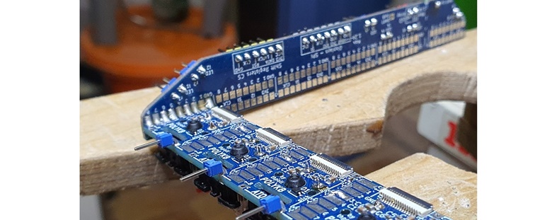
Any `Atom` can be directly soldered to the next `Atom` without any wire. That also works for the `Connector` which can be solder to the first `Atom` in a 90 deg angle:
The `Connector` contains the shift registers used to pick the right `CS` line to control the displays individually.
Right now there is a `Connector-R` and a `Connector-L` so that we can make a row of up to 16 `Atoms` without any gap. The first 8 `Atoms` are controlled by the `Connector-L` (of course on the left side) and the next 8 `Atoms` by the `Connector-R` (you already know it - on the right side).
The only important part is that the 8 `CS` lines (all of them) should NOT be soldered together in the middle, you should even better file/rasp of the edge in the middle to make sure there is no electric connection. The rest of the pins can be connected. Multiple `Connectors` also need to be chained so that the `Shift Out` pin from the previous `Connector` is wired with the `Data In` pin of the next one.
That's the theory, next time I will post some more facts on the hardware assembly.
Discussions
Become a Hackaday.io Member
Create an account to leave a comment. Already have an account? Log In.