It's been a while since I wrote a log. In this log I will tell you what happened to the design in the past months.
BYPASS
The design has a few buffers that implement the "bypass". This can place the address registers on the databus, so we can inc/dec them, or store them to T and then to memory. This is also the path to store the program counter (pch/pcl) for a CALL instruction. And it is used to add the offset to the PC in case of a branch.
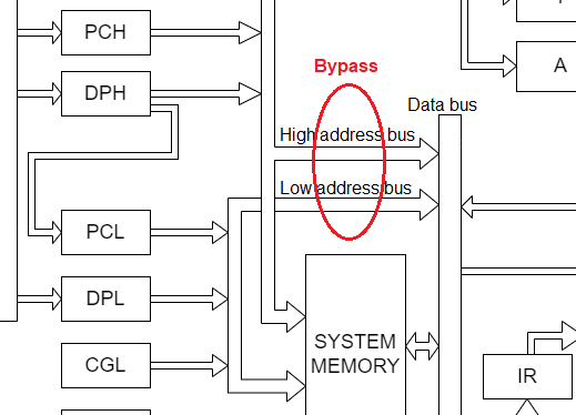
As always, I was looking for components to remove, to get a low-component-count design. And indeed, we can do without the buffer for the low address bus ! We can simply put a 1-to-1 table in a zero page of memory, and an access to this table will give us the register value on the databus. The high address bus must be 0 to access this table, that it is already an existing function.
We have 8 memory banks, so there is a maximum of 8 zero pages, enough space in zero page. One of the zero pages already has a table for right-shift.
For the high byte, this is less useful, since the table would be scattered through memory, occupying one byte in every page. That is not a good idea.
But... the only register that we need from the high bus is PCH. And the PCL bus is not loaded from the result bus, but from the DPH register (in this picture, that is. It was later changed to come from the T register).
If we modify it, and load the PCL register from the PCH register, we can access the PCH contents by loading it into PCL first ! In fact, when we write a new value to PCH we will at the same time (with the same signal) write the old PCH contents to PCL.
For doing a jump, first write the LSB to PCH, and then write the MSB to PCH (that will move the LSB from PCH to PCL). And for a CALL, first save the PCL address through the 1-to-1 table, via the ALU, to T. T is then stored to the stack. After the LSB of the subroutine address has been written to PCH, the old PCH is in PCL and can now also be saved to stack.
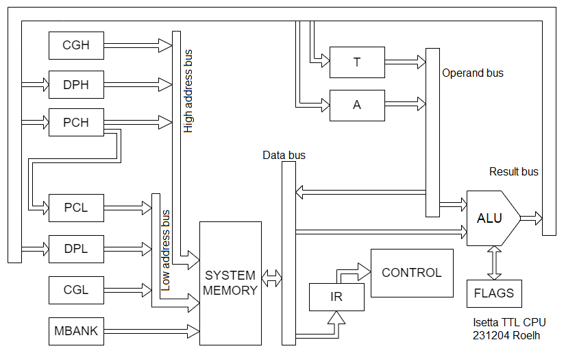
The control signal for the bypass is obviously no longer needed. Used it later to double the amount of RAM-based registers.
The 1-to-1 table in RAM is built by microcode, directly after reset, in the same loop that fills the right-shift table.
Changes for this were done in the simulator and the microcode generator.
SPEED
In october I did some timing calculations, using the typical values for 74AC logic. (These typical values are only in Fairchild datasheets, not in the Texas Instruments datasheets).
I was a bit surprised to see, that with some measures, the clock speed could be doubled to 12.5 MHz !
We would need a 10nS RAM. Circuits in the address bus needed a few changes to make it faster. One of the address signals (for the CGL register) came from a 74HC238 1-to-8 decoder that had a quite big delay. It was used to extend the number of memory-based registers. This way of extending the number of registers was dropped (replaced by a directly available microcode control bit). This HC238 also delivered a signal to select SUB and a signal to select DEC in the ALU. This could be changed to a single signal for both SUB and DEC. Other functions in the HC238 could also be solved in a different way. The HC238 could be removed.
The circuits for the flags had to change, in the design the CY-out of the adder sometimes had to pass four devices before a flag result could be clocked-in in its register. The flag system was changed such that the adder-cy-out is used at only a few places. The condition-selector can choose it, and in a group-1 instruction it can be put into the C flag. The adder-cy-out now only has to pass 2 devices. The last of these is a 74HC4053 analog switch, that is slow in switching to the other channel, but relatively fast to pass a signal. Since the switch channel can be setup at the start of the cycle, it is expected to be fast enough.
The adder-cy-out signal is called TC (temporary carry) in the microcode. For group 1 instructions, this signal is stored in a register, to make this signal accessible to later microcode instructions, this register output is called DTC (delayed temporary carry). This signal DTC can now also be chosen by the condition selector (after shuffling some of its inputs).
Today I uploaded a new schematic to the file section, that also mentions the timing of the relevant signals. The critical path takes a calculated 74 nS, so that will be fast enough for the new 80 nS cycle time.
Changes were needed in the simulator and the microcode.
There were several other changes, too many to mention them all.
Discussions
Become a Hackaday.io Member
Create an account to leave a comment. Already have an account? Log In.