The schematic capture and PCB layout were done with KiCAD, and PCBs are in fab at OSHPark. They are 100% SMT, but should be easily hand assembled as the passives are all 0805, and the ICs are SOT23-5 and SOIC 14.
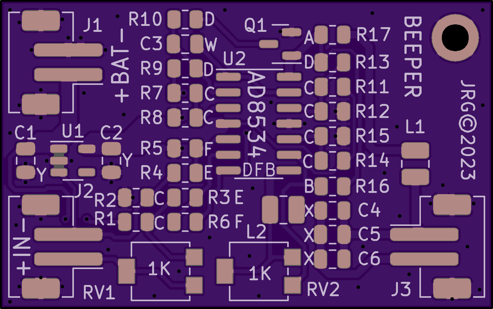
Inspecting the top of the PCB layout a few things should be noted. As this project was potentially to be built by others, I increased component spacing a bit to ensure every component had it reference designator nearby and unambiguous.
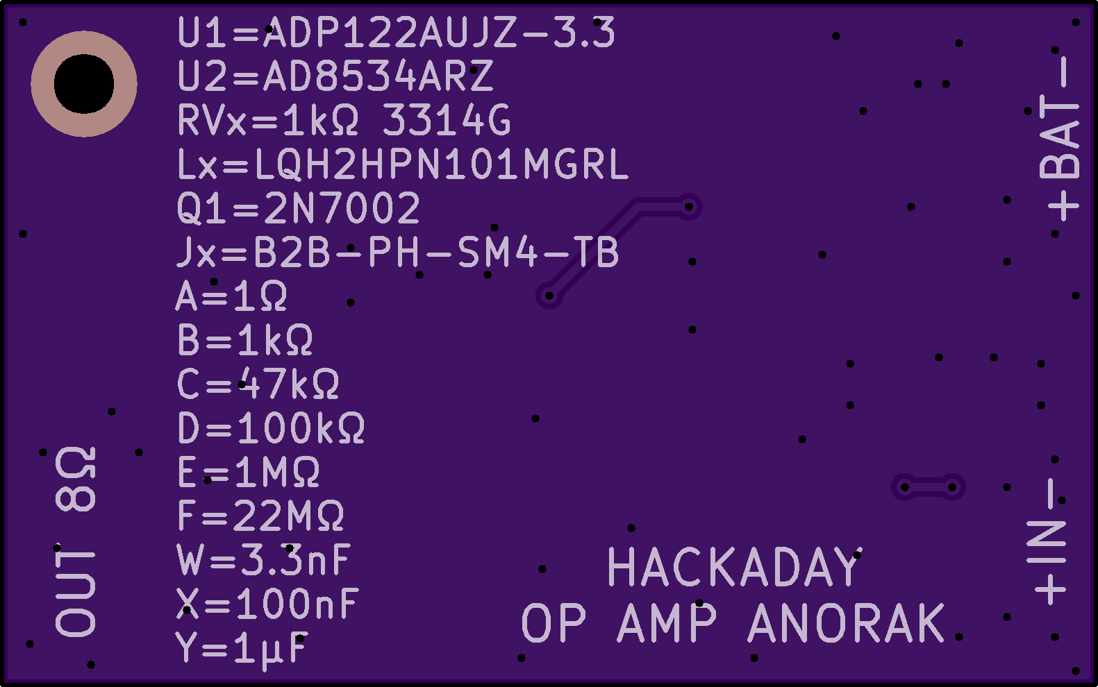
Also, note the 0805 components all have a letter next to them as well. If you look at the PCB bottom, there is a legend providing values or part numbers for every single component on the PCB. I wanted to ensure that if I or anyone else had a blank PCB in their hands it could be built without the aid of a schematic. I wish I did this more often!
Beneath the op amp U2 AD8534 are the initials DFB, a good friend and the designer of the AD8534.
Discussions
Become a Hackaday.io Member
Create an account to leave a comment. Already have an account? Log In.