 Clyne
ClyneThe add-on board’s revised schematic and board layout are practically complete; the next couple of logs will go over the significant changes in the hardware design for this next iteration.
The primary changes in the schematic come down to the filtering and conditioning of the input and output signals given the new signal specifications. Design tips and strategies were taken from multiple resources to maximize accuracy and minimize noise. This highlights the best piece of advice I can give to those designing circuits and schematics: use all of the resources at your disposal. Nearly all datasheets for integrated circuits (ICs) include detailed “Application” sections that show circuits, discuss component selection, provide calculations to meet design parameters, etc. Following these instructions will ensure a sound design. Major manufacturers also have vast collections of application notes that cover a wide array of electronics design topics. These can be found on their websites, or simply by searching the internet. There’s no reason not to work off of proven designs and knowledge when you can.
Input signal
Previous designs of the add-on board used basic inverting amplifier configurations to achieve the simple goal of scaling signals to the desired voltage ranges. Amplifier ICs were chosen solely on the basis of if they can achieve this goal. Later on, slight changes with passive components were made to reduce high-frequency noise.
For the next design, I turned to an application note from Texas Instruments (TI) on “Active Low-Pass Filter Design” and the accompanying Filter Design Tool. Given the project’s new specification on maximum sampling rate, a second-order active filter could be used to achieve an optimal signal-to-noise ratio. The max rate of 96 kHz was rounded up to 100 kHz for simplicity.
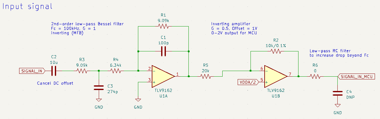
A Bessel filter was chosen to avoid gain overshoot below the cut-off frequency, at the cost of reduced attenuation performance. To compensate, the Multiple Feedback (MFB) architecture was used to optimize the high-frequency response; placeholders for an additional low-pass filter stage (R6 and C4 in the above photo) were also added in case increased attenuation is necessary. MFB also has reduced sensitivity to component variation, allowing for some component cost savings.
The Bessel filter is preceded by a series capacitor that cancels out any DC offset in the incoming signal. The previous design instead canceled the offset by feeding the ground of the input audio jack into the differential amplifier; however, this approach was not proven to be sound or “correct”. A series capacitor is an easier and safer choice. The value of 10uF is fairly arbitrary, and will be adjusted during testing if needed.
The second stage of the input signal path is a simple inverting amplifier, as the MFB architecture of the first stage is also inverting. The second stage is also used to add a DC offset to the signal, bringing it into the acceptable voltage range for the ADC.
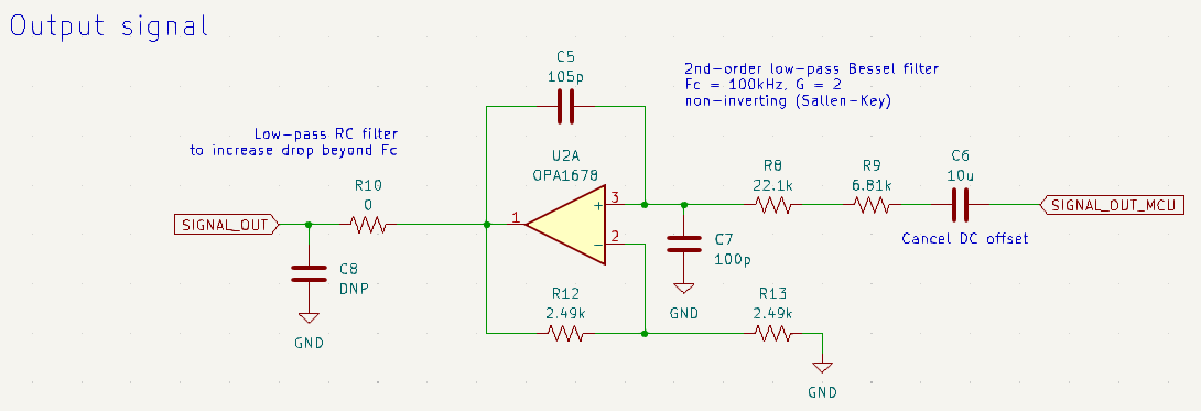
Output signals
The output signal (and signal generator output) uses a Bessel filter just like the input signal. A Sallen-Key architecture is chosen this time though, primarily for the fact that it produces a non-inverting configuration. This means there only needs to be one active stage in the output path. The drawback is a potential reduction in high-frequency response; the optional low-pass RC filter is included in case this reduction is worse than desired.
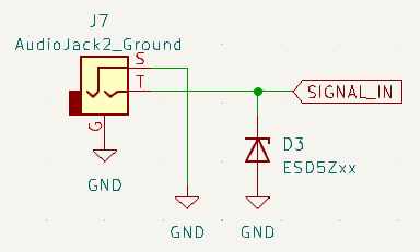
ESD protection
This design introduces ESD (electro-static discharge) diodes on the audio jacks and USB port. ESD can occur on any component that interacts with the outside world (e.g. human touch), so it is good practice to include this kind of protection. In a worst-case scenario, unprotected ESD could damage components on either of the add-on or microcontroller boards.
The choice of diode is flexible as long as the diode does not breakdown within the normal voltage range of the line that it is connected to.
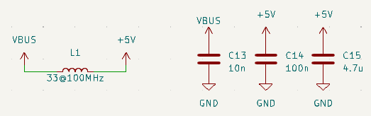
Source supply filtering
Finally, some passive filtration was added to the source power supply (5V from the USB port) to prevent it from being a possible noise source. The inductor and capacitors work to create a low-pass filter, with the variety of capacitors combating different frequency ranges. The chosen component values are based on existing designs (and following advice from this blog post) and are open to adjustment during testing.
Discussions
Become a Hackaday.io Member
Create an account to leave a comment. Already have an account? Log In.