 Clyne
ClyneThis log will give an in-depth report on the testing and ciruit alterations that were made to get the analog input signal circuit working as desired. The alterations were able to be kept to simple component swaps, so future boards can be ordered with just a few changes to the bill of materials.
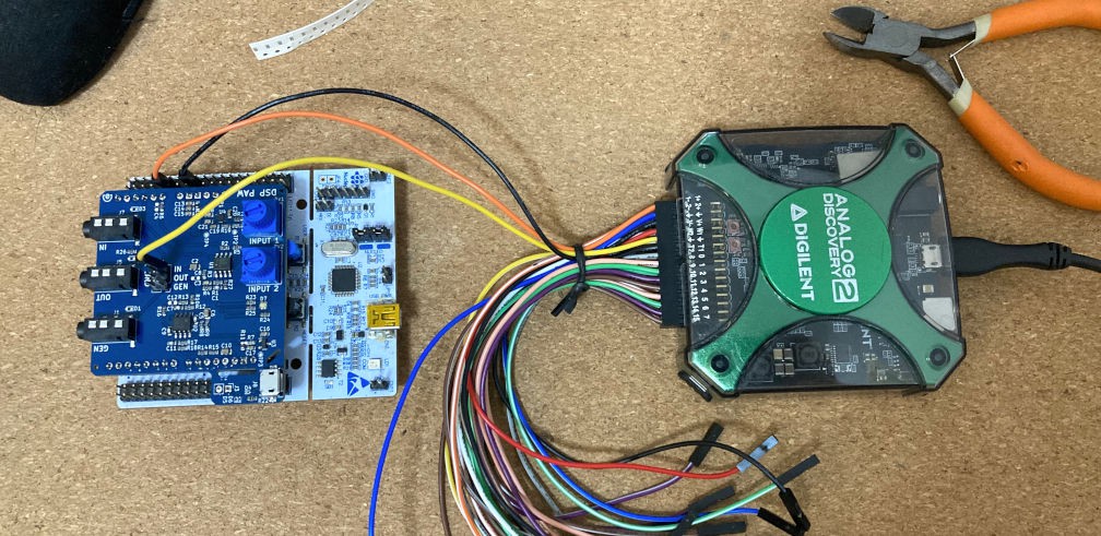
To analyze the signals, I hooked up my Analog Discovery 2 to the NUCLEO and add-on board. For the input signal path, the Discovery's waveform generator was connected to the add-on board's signal input and an oscilloscope probe was hooked to the ADC pin that receives the conditioned signal. A third wire gives us a common ground:
A couple of power supply observations
Once the add-on board was connected to the NUCLEO, some of the add-on board's power supplies were not behaving as expected. First, I noticed that the add-on board's +5V and -5V test pads were reading voltages around +/- 3.6V. The add-on board gives USB power to the NUCLEO through its VIN pin, and expects the NUCLEO to give that back on its 5V pin; however, revisiting the NULCEO's schematic proves that this is not the case.
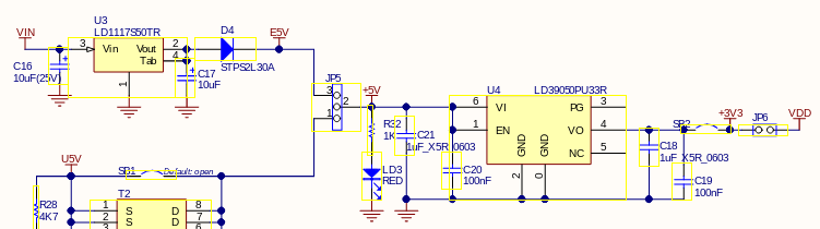
The NUCLEO puts VIN through a 5V linear regulator and a protection diode before the "E5V" net, which is passed to +5V through a jumper. Both of these components create significant voltage drops for the power going through them:
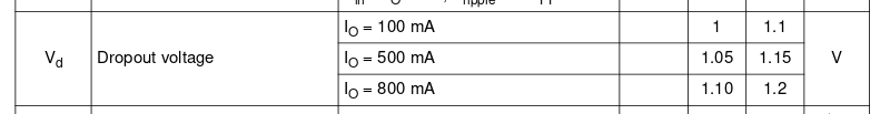
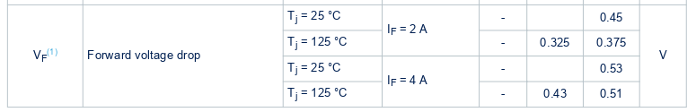
Take the 5V input voltage and subtract the 1V and 0.4V drops and you get 3.6V -- just what we're measuring. Ideally, the add-on board would be re-routed to give its 5V USB power directly to the 5V pin, but for now we can get by since the operational amplifiers (the only components using +/- 5V) just need +/- 2V to properly handle our signals.
Analog voltage reference
I also verified that 2.048V analog voltage reference now that the NUCLEO board was connected, and measured... 3.3V. That would be the NUCLEO's default reference voltage, with the schematic showing that a jumper handles this connection. We'll need to desolder a jumper on the bottom of the NUCLEO board.
This might present an issue going forward, since it means users will need to be comfortable with (and have the means for) desoldering this jumper. The 2.048V reference is far less noisy than the NUCLEO's 3.3V, so this decision will have to take some thought.
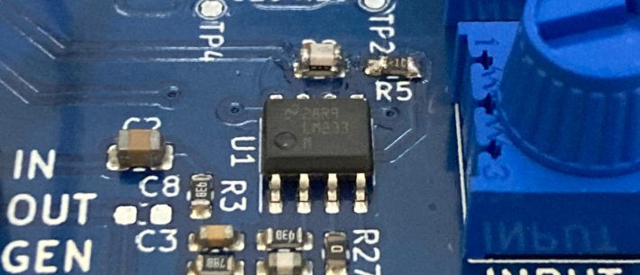
Apart from this connection, the resistor divider on this reference that's used for shifting the input signal above negative voltage is incorrect. The division needs to be by four, not two as the board was accidentally designed for. I should have caught this before ordering the boards by comparing schematics with the previous iteration, but oh well... the fix is an easy resistor swap on R7 (from 10k to 30k):
Input signal analysis
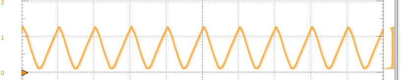
With the above out of the way, it's time to turn the oscilloscope on and run some simple tests. We start with a 0V signal to check noise and offset (+/- 2V is converted to 0 to 2V, so a 0V input should read on the ADC pin as 1V):
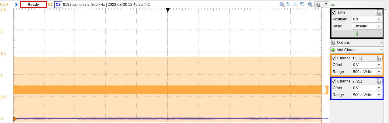
Sadly, this is not a clean signal or a 1V signal. A closer capture shows that we're getting a sine wave with a 1.4V swing at 1.4 MHz.
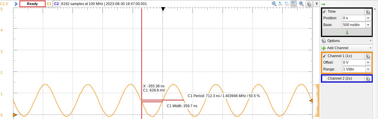
This is a clear indicator that one (or both) of the opamp stages are unstable and creating oscillations with their feedback networks. The remedy is often found with capacitive adjustments: we can either balance the input and output capacitance, or we can add capacitance to the feedback network to create a delay that stabilizes the feedback. I tried adding output capacitance first, and while that cleared the oscillation it also created a low-pass filter that ruined signal inputs above 1 kHz. Adjusting the capacitance to allow higher frequencies would lead the opamp back into instability.
So, we go with the feedback capacitor. A capture of the first stage opamp's output showed a stable signal, indicating that it was the second stage creating the oscillation. This means that capacitor would stack onto R2, and after some trial-and-error (touching through-hole ceramic caps to R2 while monitoring the output) a value of 100pF was chosen. The clean output can be seen in the following scope captures.
Gain and offset adjustments
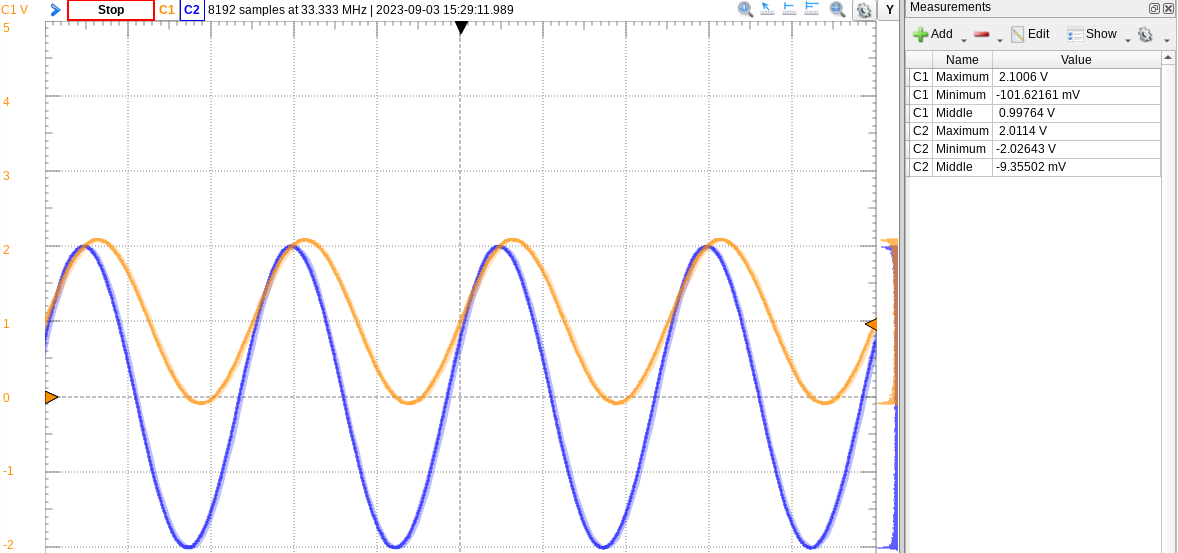
With the opamp filter stabilized, we can now compare the overall circuit's output against an input sine wave. I set the input amplitude to 2V so that we can check the full range of supported voltage.
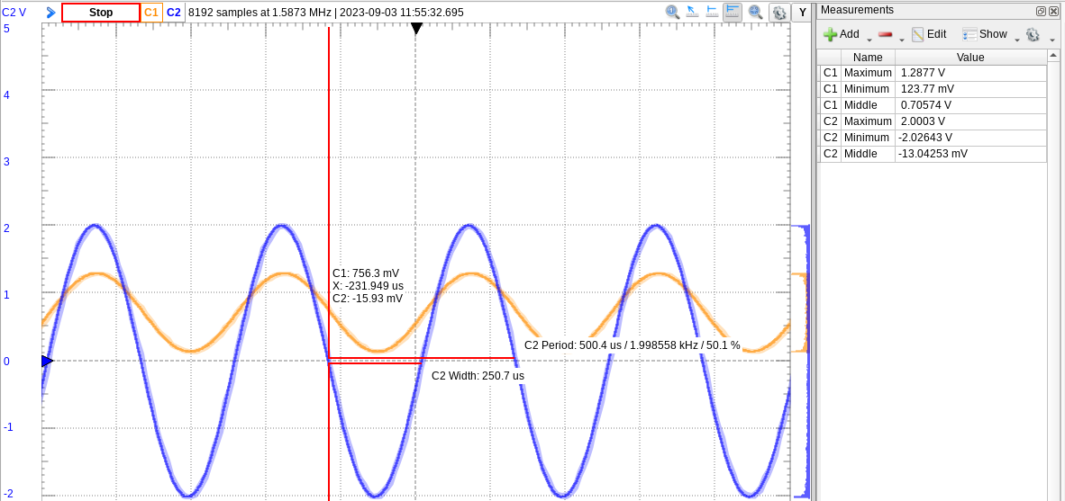
There are two problems to tackle here: first, the output onto the ADC pin is not swinging from 0V to 2V as was expected; second, that output is only at an offset of 0.7V when 1V was expected. I went after the incorrect gain first, since there's a chance that it is also affecting the added offset.
The input signal's gain is adjusted by the second filter stage which is a basic inverting amplifier with G=0.5. In the above capture, we're only seeing a measured gain of 0.29. While the inverting configuration does allow for gains less than one (G = -Rin / Rfb), some extra research has shown that gains less than unity (i.e. 1.0) are likely to go unstable, possibly causing this problem. A separate thought of mine wonders if the first filter stage is influencing the gain: if we consider the first stage's feedback resistor of 9.09k as additional input resistance, the gain of the second stage theoretically becomes 0.34 -- much closer to 0.29.
To test both possibilities, I swapped the second stage's input resistor to 10kOhms. This either creates stable, unity gain, or a theoretical gain of 0.52.
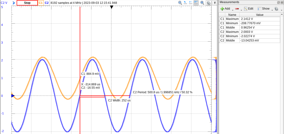
The measured gain has increased to 0.58, suggesting that input resistance from the first stage is most likely factoring in. We now get a swing slightly beyond 0 to 2V, and the offset has also increased for the better to 0.963V.
For the signal offset, I inspected the circuit's initial series capacitor next. It's meant to cancel DC offsets in the input signal, and does a good job at that, but it hat also turned out to introduce a constant offset itself. Before this capacitor, the input signal has a "middle" of -13mV; after the capacitor, this drops to -64mV. That drop remains constant when the input signal's offset is adjusted.
The difference in drop is 50mV, which is very close to the difference between our current output offset of 0.963V and the ideal 1.0V. After removing the capacitor and shorting its pads, we achieve an output offset of 0.997V:
The span of the ADC signal has also closed in on the 0 to 2V range, though we're still seeing peaks with negative voltage. There's a risk that this will damage the ADC over continuous use, so a slight reduction in gain would be beneficial. At this point, I turned to the Falstad Circuit Simulator to simulate the two opamp stages. This would both confirm that both the current design is sound, and allow me to determine the final change(s) to perfect the output.
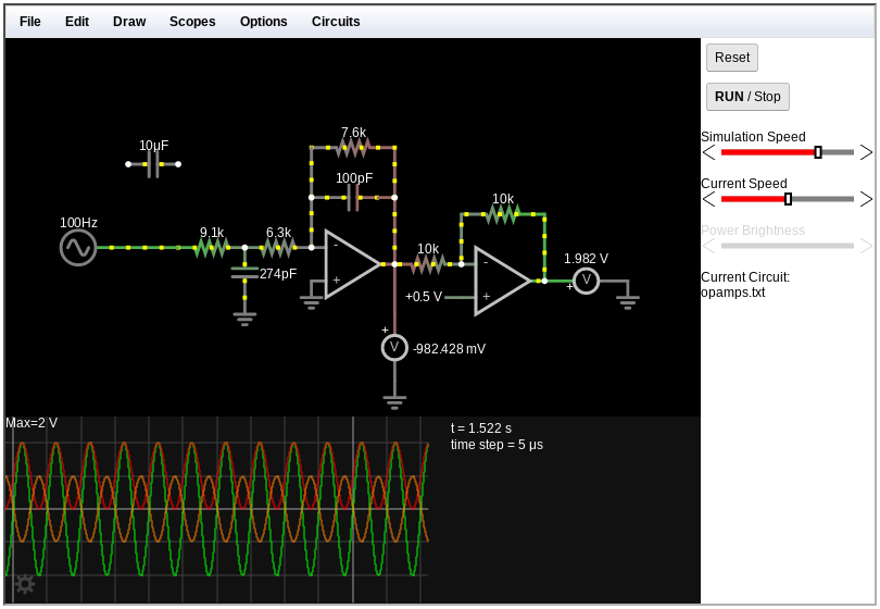
With some trial-and-error, I found that slightly decreasing the first stage's feedback resistor would produce an ideal gain factor. I have 7.5kOhm resistors handy, so I swapped one into the circuit and checked the result:
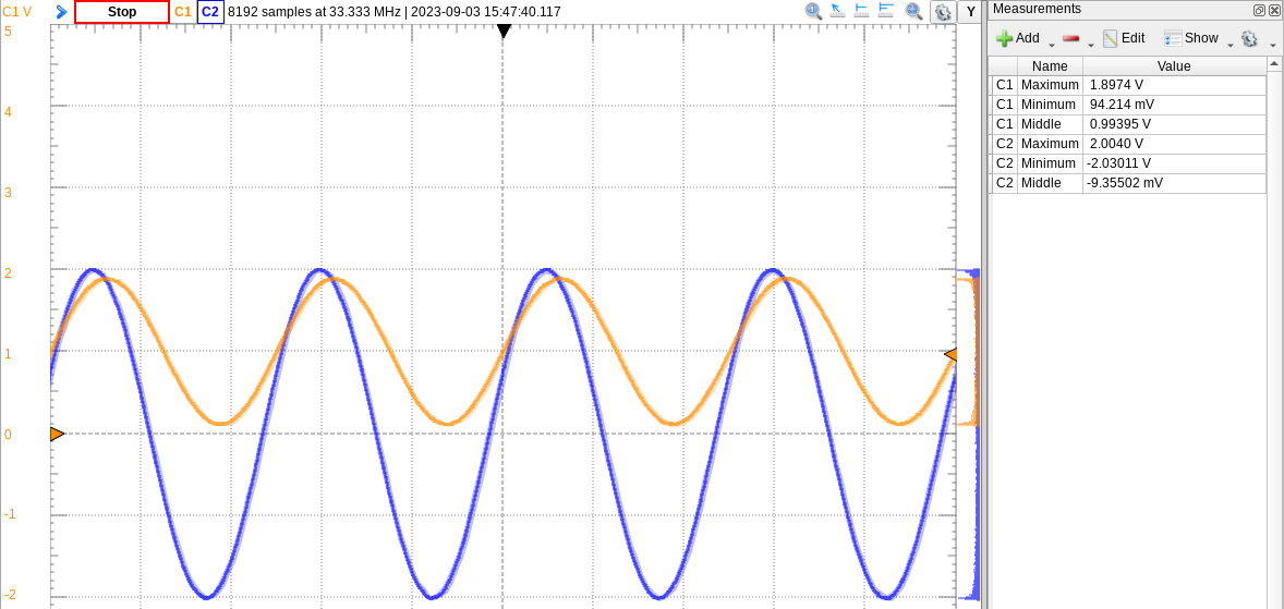
Finally, we reach acceptable performance. The gain could still be improved by ordering a different feedback resistor to bump the gain up a little more.
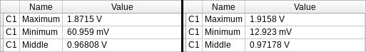
Towards the end of testing, I noticed that our measured results may not be as far off as we have observed. The two tables below show measurements of the ADC waveform with (left) and without (right) the second probe on the blue input signal -- improvement is seen in every measure. Even better, the below numbers are from a test with the DC-blocking capacitor added back in, so that's one less change needed for future boards.
Frequency analysis
For a final test, let's confirm that the input signal path can accommodate the entire frequency range that we wish to sample. Our upper bound is specified to be 48 kHz, since our highest sampling rate is 96 kHz. The lower bound is no more than 20 Hz to allow all human-hearable frequencies; going lower is welcome, but issues may arise from circuit capacitance and DC blocking.
I used a Fourier transform to capture the strength of the input signal as I swept it from 48 kHz down to 10 Hz. The peaks throughout the graph are the frequencies that I tested:
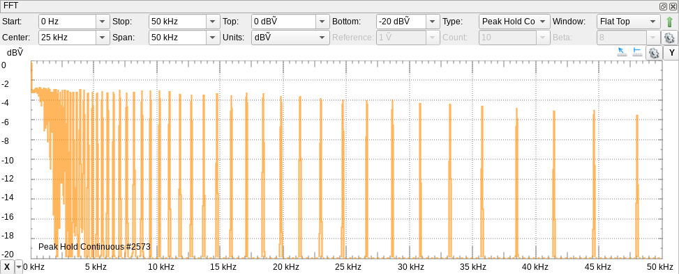
The signal proves to be strong across the spectrum, just barely dropping by -3dB at 50 kHz. This performance is just right for our needs.
Conclusion
The input signal path has been tested and adjusted to reach the range of performance this project needs. The next step will be to validate the output signal path, which I'm going to separate into another project log since this one has become so long.
Once the output is tested, we'll get to run some algorithms through the new board capture the results. I'll most likely do this in a video to have a true "demo" of the project.
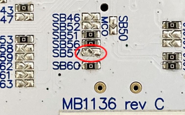
As a final note, here is a picture and summary of the changes made to the board so far:
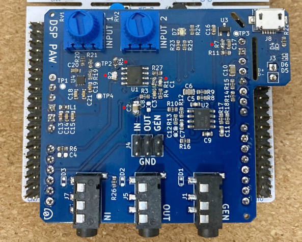
- R7: Change to 30 kOhm for correct voltage reference division.
- R1: Change to 7.5 kOhm to reduce gain of first opamp stage.
- C2: No change. Was initially removed to improve final signal offset, but adding this back in at the end saw no performance loss.
- R5: Change to 10 kOhm to increase gain of second opamp stage.
- R2: Stacked 100 pF capacitor on top of the resistor to stabilize the second opamp stage.
Discussions
Become a Hackaday.io Member
Create an account to leave a comment. Already have an account? Log In.