 Clyne
ClyneThe latest iteration of the add-on board saw a major step towards a final design that I would feel comfortable selling to interested users. As previous project logs have shown, the design still had numerous component substitutions and circuit rewirings to be made. Since the board's circuits were all brought to an acceptable state I have added these fixes back into the schematic. With a couple of other design changes, I have arrived at (what I truly hope will be) the final add-on board design that is production ready.
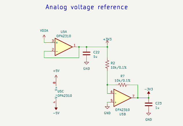
Analog voltage reference
Despite the effort that has gone into bringing a high-accuracy 2V reference to the add-on board, I am making the decision to return to relying on the NUCLEO's provided 3.3V reference. Firstly, this will eliminate the requirement of removing (desoldering) a jumper resistor from the NUCLEO board. Second, a closer look at the microcontroller's documentation reveals that VDDA should never be less than VDD, meaning the use of a 2V VDDA is technically unsupported (although it has worked well for the prototypes).
As a final solution, the NUCLEO's provided reference will be buffered to prevent sagging from the add-on board's load. We will also generate a negative reference voltage for use with the input signal circuit; this should both improve input accuracy and prevent the ADC input from exceeding its specified range.
Input signal circuit
In the last design iteration the input signal path produced an unstable, oscillating output that required multiple changes to fix. It is still unclear what resistance is driving the second stage's attenuation factor as well as the overall stability of an inverting amplifier with gain less than one. I've redesigned the input path entirely to create a circuit that is well-defined in its behavior:

The first stage has been modified to use the same Sallen-Key architecture as the output amplifier circuits. The slight loss in performance is outweighed by the reduced design complexity and the non-inverting output that makes the revised second input stage possible. This second stage uses a surprisingly simple voltage divider to achieve both the desired attenuation and offset to the positive voltage range: the lowest input voltage of -3.3V becomes 0V, the midpoint of 0V gives 3.3V/2, and the maximum of +3.3V remains at 3.3V. A buffer takes the result through a final low-pass filter that was added during testing before entering the ADC.
Other changes
Apart from these two major changes are the small fixes I made during the prototype testing to stabilize the output signals and a fix for the parameter knobs to use the proper source voltage. I am also switching the two output circuits to use individual amplifier chips; this way, the amplifiers can remain close to the pins that the signals originate from which minimizes noise being picked up by long traces.
The revised schematic is currently available on a "rev2" branch of the project's repository. I have a lot of confidence in this new design, and look forward to testing it out once I finish its layout and order a few prototype PCBs.
PS: Self-assembly
This time around I may also do component assembly myself to both save on cost and to order parts directly from Digikey where I can ensure I get the exact components in my BOM. When I ordered assembled prototypes through JLCPCB, I had to make compromises on component values, tolerances, and even an amplifier choice to make use of the their available stock. By ordering components myself, I'll make sure the resulting prototype is designed exactly to what the schematic calls for.
Discussions
Become a Hackaday.io Member
Create an account to leave a comment. Already have an account? Log In.