Close
0%
0%

DIY LM358 RRIO OpAmp

If opamps are super useful, RRIO opamps even more.
.

Similar projects worth following
120 views
As I only have jellybeans IC, let's build a RRIO out of LM358 and understand how it is done internally on native ones.

This project is an attempt to understand how RRIO opamp work internally, and to replicate one with very common components.

Goals

While the learning part is the bootstrap of the intention here, we want to have a real opamp at the end of the journey.

Main objective

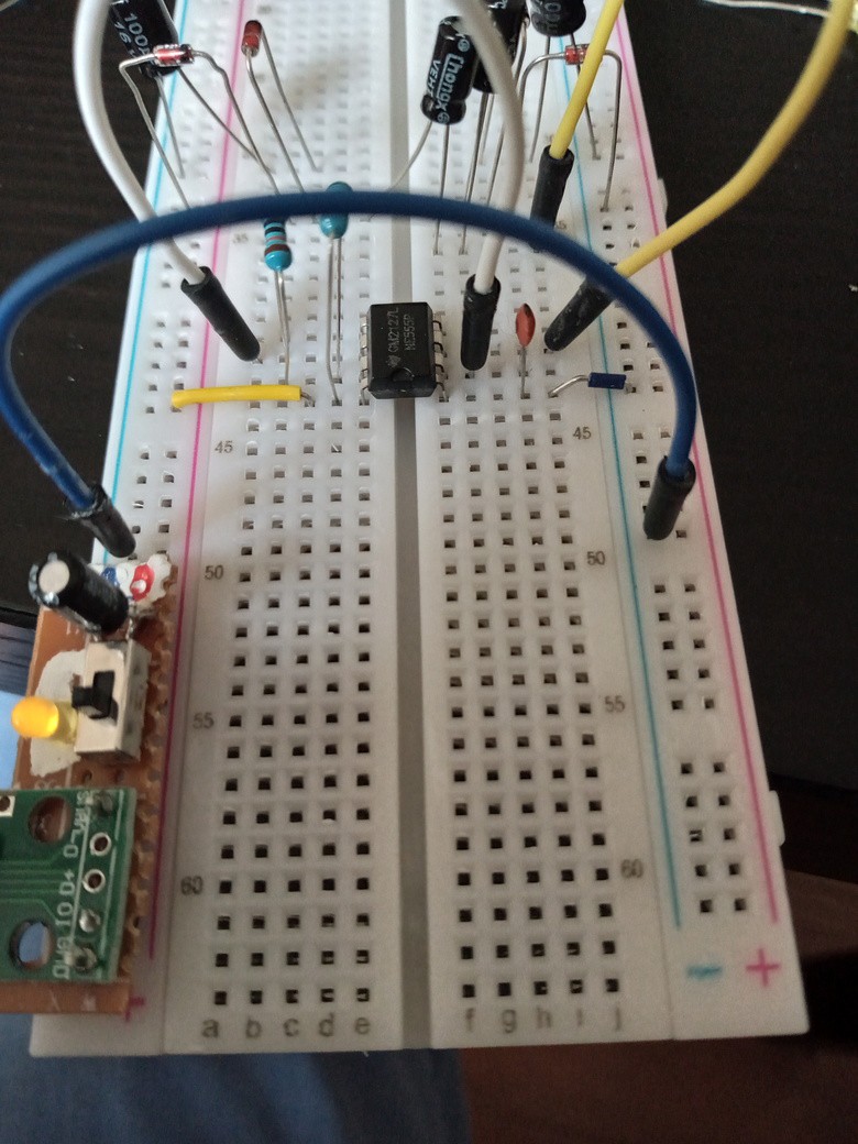
The main design goal is to leverage components as common as possible. That includes passive components, such as resistors & condensators, but also very common IC. Which includes ones like the LM358 for opamps of course, but also the NE555, so it could even participate in the now-defunct NE555 challenge.

Using another LM358 instead of a NE555 might be interesting for the sake of staying withing the opamp challenge, but it might go against the secondary objective. 

Secondary objective

An SMD version of this circuit should be aimed to be a pin-compatible DIP-8 version of the most common dual opamps for an elevated challenge. If DIP-8 proves to be too complex, we can aim for a pin-compatible quad-op in a DIP-14 format.

Design

The design here is very easy.

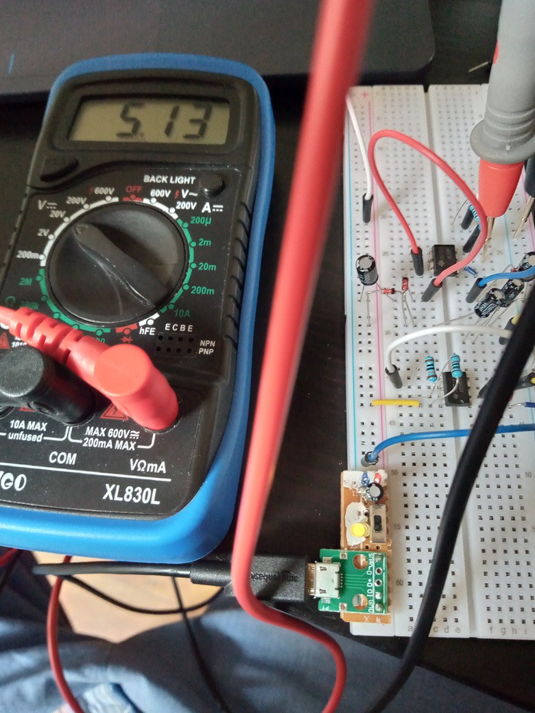
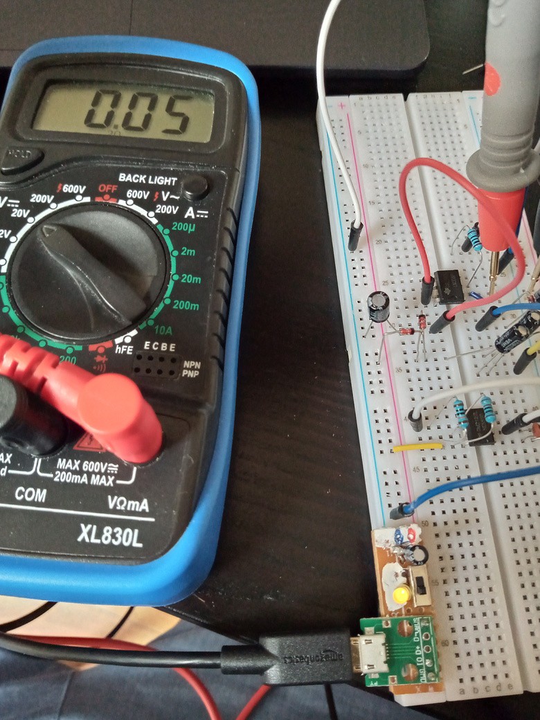
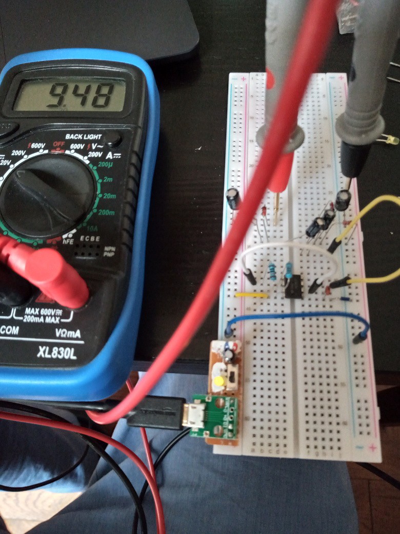
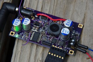
To be able to put the LM358 in RRIO mode, I'm simply cheating and supply it with single voltage source that is has a little more amplitude than the main voltage source.

This is to overcome the various voltage drops that are inherent to the internal LM358 construction.

The simplest way to achieve it is a capactive charge pump. This is incidentally the same way that many RRIO achieve input rail-to-rail. Output rail-to-rail is usually done with a CMOS buffer instead of the charge pump, in order to limit the current need on the pump and be able to fit it directly inside the die of the IC.

I don't plan to add the CMOS output buffer, but instead generate a charge pump powerful enough to also be able to drive the opamp load directly.

  • 1 × LM358 Operational Amplifier IC
  • 1 × NE555 Temporisation IC
  • 4 × 1N4148 Signal Diode
  • 2 × 100uF Polarized Capacitor
  • 2 × 1uF Polarized Capacitor

View all 6 components

  • Adding the LM358

    Steve Schnepp05/07/2023 at 14:31 0 comments

    Let's finally add the LM358 to the mix.

    Without Load

    It works quite well without any load.

    Positive & Negative outputs are within 50mV of the input with a simple voltage follower.

    With Load

    As expected, with some load, the voltage isn't that great : 3.3V only at 2.4mA, which isn't surprising, given the output of the charge pump.

    Conclusion & Improvements

    My initial idea didn't work as well as expected. Without load it is perfect, but as soon as some load is added, the voltage drops. 

    But the good findings are that the charge pump is the weak link here. So, if it is improved it should be fine.

    I'll planning to try 2 improvements:

    • Using a LMC555, which is the CMOS version of the NE555 as suggested in the comments by Ken Yap.
    • Using a CD4069 CMOS buffer to achieve the same effect than using the LMC555.

    Once I'll manage a stable output even with the max expected load from the LM358, I'll aim to miniaturize on a PCB.

  • Breadboard Time for the Charge Pumps!

    Steve Schnepp05/07/2023 at 13:23 0 comments

    Simulation works nicely, now let's try it out for real. 

    As Ken Yap nicely commented, there is a strong voltage drop in the bipolar NE555, typically 1.7V. The usual way is to leverage a CMOS version such as the LMC555, but as I'm aiming for very common components, I'll use only regular NE555.

    Building the charge pumps

    The charge pumps are not hard to build. I'm using a simple breadboard, and a very simple DIY USB powering for 5V.

    Testing the outputs

    Now, it is time to test the 2 voltage outputs.

    A very nice 9V and -4V.

    Issue is that it doesn't hold the voltage as nicely with some load. I tested with a yellow LED in series with a 1k resistors and it falls to 4.5v with a current of 2.4 mA (2.4V across a 1k resistor).

    Anyway, let's try with the LM358 now.

  • Everything starts in a simulator

    Steve Schnepp05/07/2023 at 12:36 3 comments

    First, I start all my designs in a simulator. I'm using the one from Paul Falstad, as it is dead simple to use, and working well enough for most of my needs.

    I'm using a NE555 to generate a dual voltage power source from a single voltage one. The pattern is very common : a simple capacitor charge pump for each voltage.

    I don't need to have a very high or low voltage, as I only need to supply a little more that the voltage drops in the opamp IC.

    Note, I also leverage the fact that the NE555 has a rather strong output, and it will be able drive both charge pumps directly without needed to use buffers. 

    The values I'm using are also rather common as it is only power-of-ten. Which are the most easy to source components.

    The diodes will be the very common 1N4148, also ubiquitous to find. Using some Schottky ones like the 1N5711 might be more efficient, but they are more difficult to source.  


    The circuit is available in the Live Simulation.

View all 3 project logs

Enjoy this project?

Share

Discussions

Kuba Sunderland-Ober wrote 06/07/2023 at 21:07 point

LM358's common mode and output range extend to ground. The 50uA output sinking capability below about 0.8V can be vastly improved by adding a current sink. It can be just a pull-down resistor, or an active bipolar or mosfet sink. Low conductance NMOS devices in the CD4007 chip make great sink current sources, and give quite a bit of an improvement. Extending the range to V+ requires some sort of a boost converter, exactly as you show. This is a neat idea!

  Are you sure? yes | no

Similar Projects

Does this project spark your interest?

Become a member to follow this project and never miss any updates