 Collin Matthews
I spent 6 months on and off trying to understand the problem, trying to find a schematic or create one, and finally in the end found a single bad resistor was causing the feedback circuit to be ~1/3 the result it should have been.
Read on to see some of the steps I took to get there.
Also - Check out the below video for a deeper overview on the internals and operation of the supply.
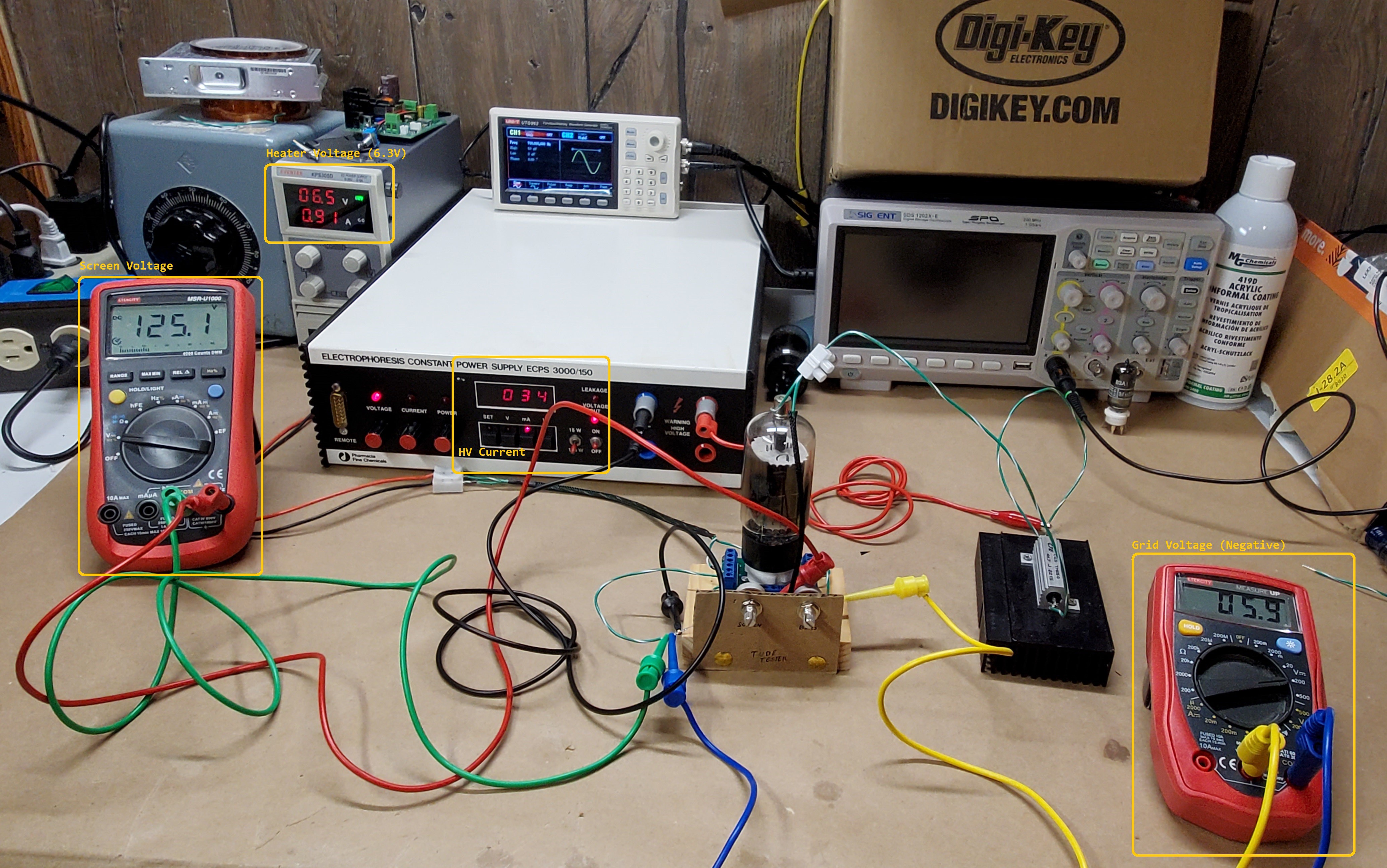
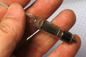
Tube Checks
As you will read below, install troubleshooting proved to be challenging, so I figured I could at least test the reference and power tubes. I thought they were good based on the supplies ability to hold regulation under load, but it has been a project I have wanted to do for a while. You can check out the results here
Surprise, the two 8086 power tubes and 83A1 reference tube were all fine. Unfortunately this pointed to an issue with the regulation circuitry.
Transistor Checks
With an accurate schematic still alluding me, I figured best to test all the transistors for functionality, since this could easily be done on a bread board due to them all being socket based TO39 packages. I used a DMM in diode mode to determine if they were PNP/NPN since I was not confident given some of the parts do not have datasheets or really any reliable information about them.
I found this YouTube video helpful with determining pin-out and type of BJT.
Unfortunately I did not take any pictures of this part, but I just took measurements of the transistor in a typical* operating common emitter circuit at different voltages and verified the collector current scaled with the base current.
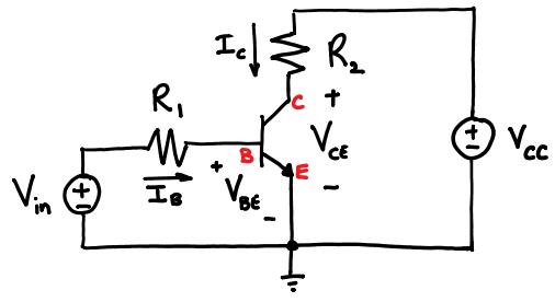
I created pages on two transistors I found with more limited information available online. Yes this was excessive, but again maybe someone will find this helpful.
Surprise again, no issues. The NPN and PNP transistors all tested out ok, and were similar in performance across multiple of the same part number.
The Control Circuit
The controls for the supply all float on the high voltage output rail, this makes taking measurements potentially dangerous. Even something like a cheap multi-meter could go up in smoke with a slip of a probe. The good news here, I found out that all the control circuitry is running when the supply is powered up, but with the high voltage switch off. This limited the available voltages to ± 260V, a slight improvement.
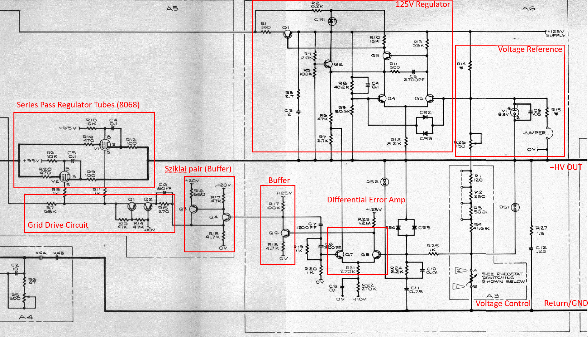
I could not find a schematic for a 412b anywhere, so I initially tried to create one by taking pictures of the top and bottom of the boards, and overlaying them in Photoshop with some small tweaks to the perspectives, this method works quite well I discovered.
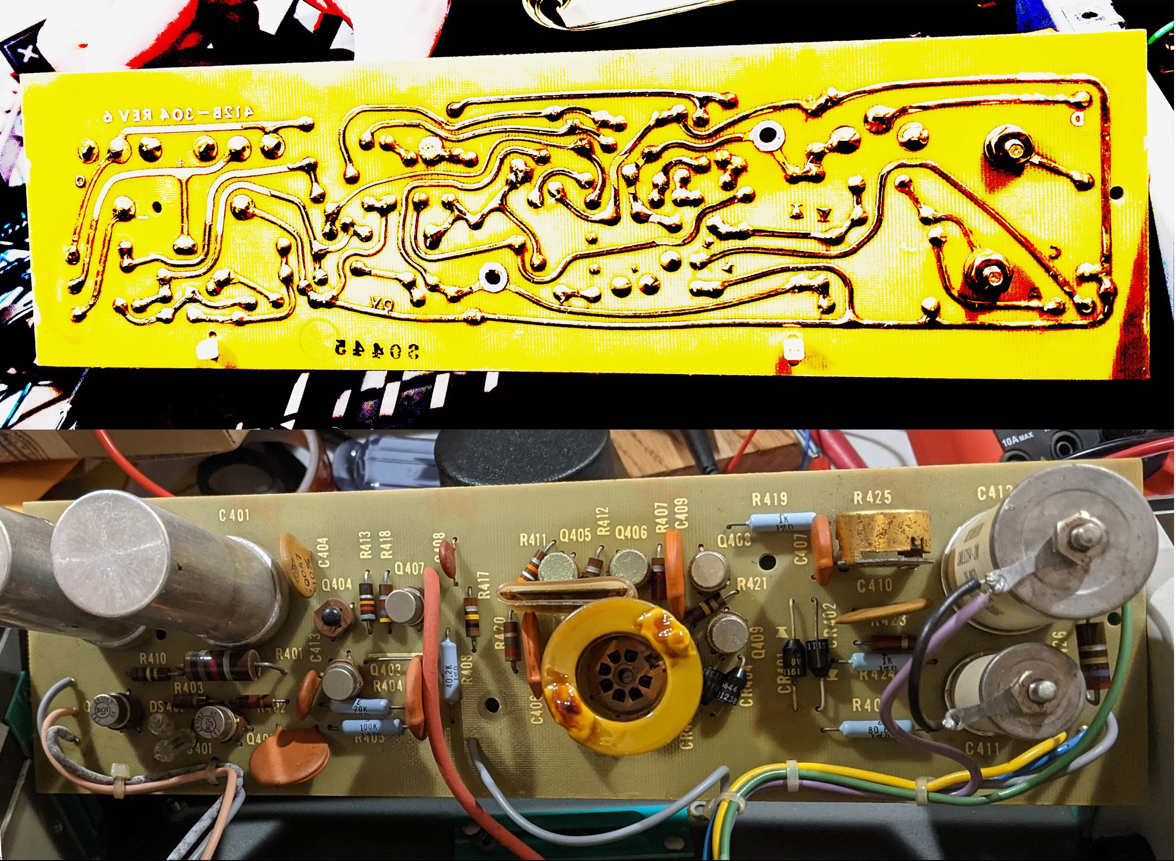
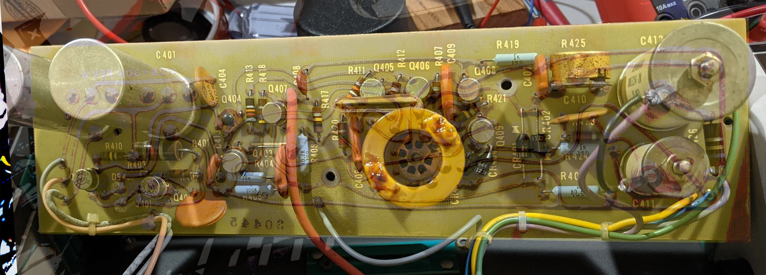
At this point I switched gears. Fluke Makes a 3kV supply (The 415b) which has a high quality schematic available online from 1966, a similar year to my supply based on the dials on the front face. I found the reference designations were radically difference, but the physical layouts were nearly identical. This gave me confidence in the following schematic, which I then marked up segments into what logically made sense to me.
The whole process of trying to generate a schematic and eventually matching this similar schematic to my supply taught me a lot about classical analog design, the voltage reference is a tube, the precision resistors looked like mica plates, the sziklai pair (I had never heard of this transistor layout before).


 Yann Guidon / YGDES
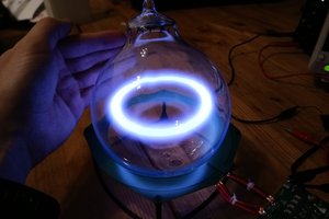
 sky-guided
 Tony
Tony
 Paul Andrews
Lovely project, I'm very glad to see that thing of beauty back in action :)