The design is simple, the idea is to stack everything over standard Arduino board layout.
From Arduino I need only SCL,SDA and GND.
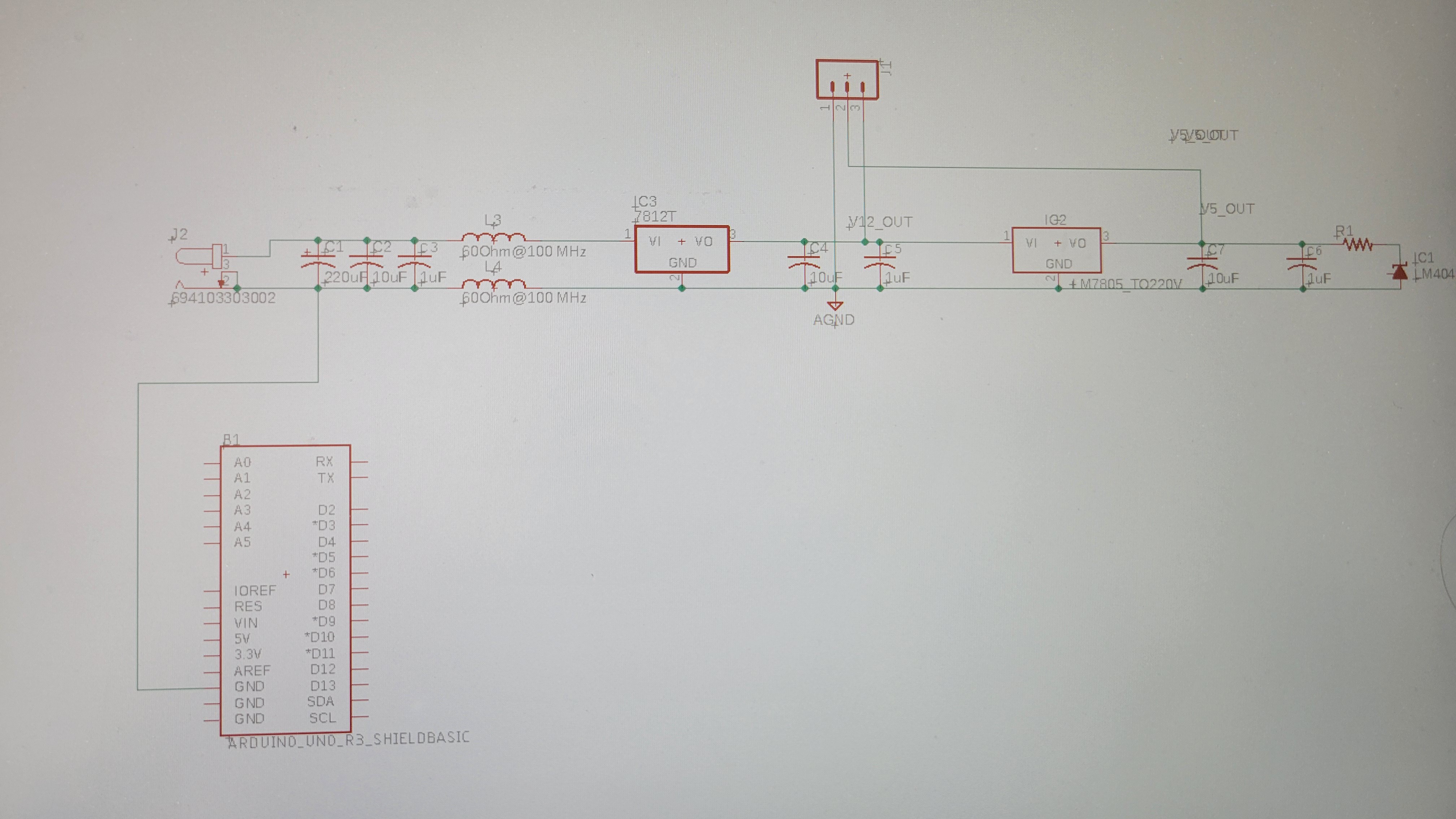
So, I will get one board for Arduino. Another one for power supply. Power supply will generate 12v and 5v only.( The double rail voltages will be created at each board that needs it). It's tempting to make the 12-(-12) and 5-(-5) voltages on the power board and route them to needed boards, but I am afraid long lines will add noise. Plus we prefer each board to has it's own voltages, this way we reduce inter component's noise.
Another observation is to use analog ground planes and not standard GND ones.
Some chips needs special layout like charge pump, so special care should be taken when designing them.
Another advantage of using stackable boards is each user potentially could choose which sensor to use.
Ok, let's start with the main board which provides rectified voltages of 12v, 5v and analog ground.
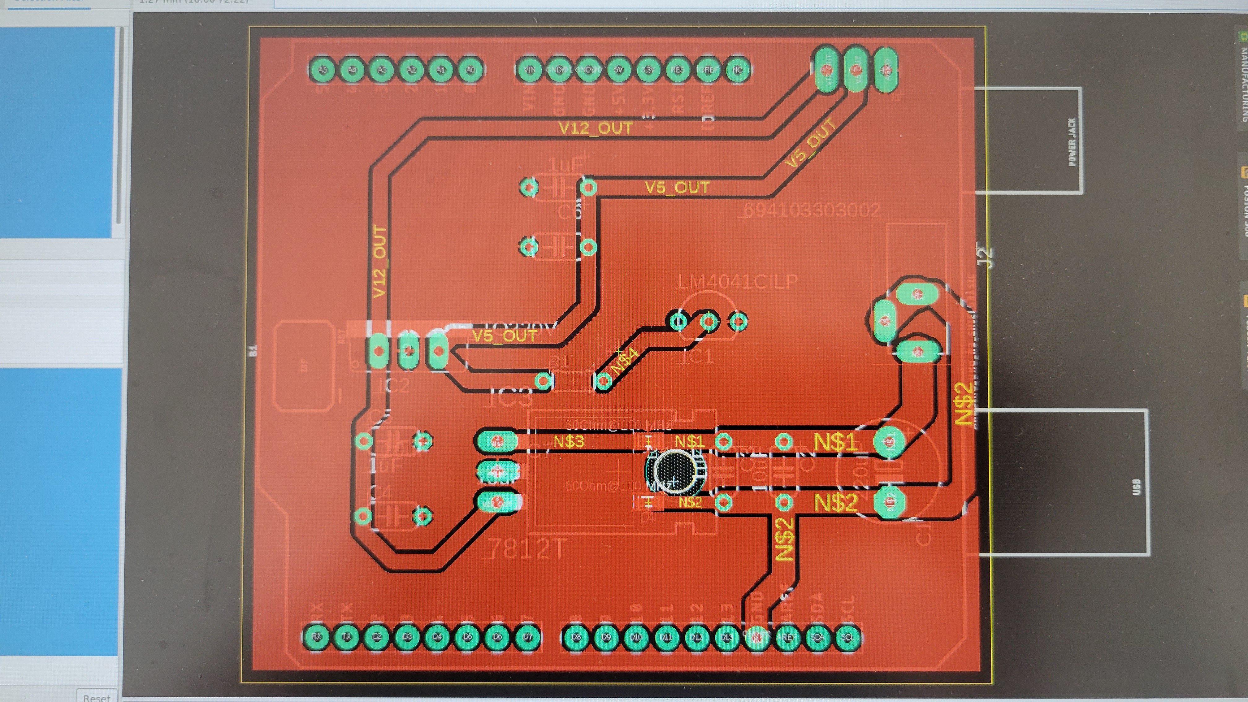
And it's getting bit messier on Arduino shield...
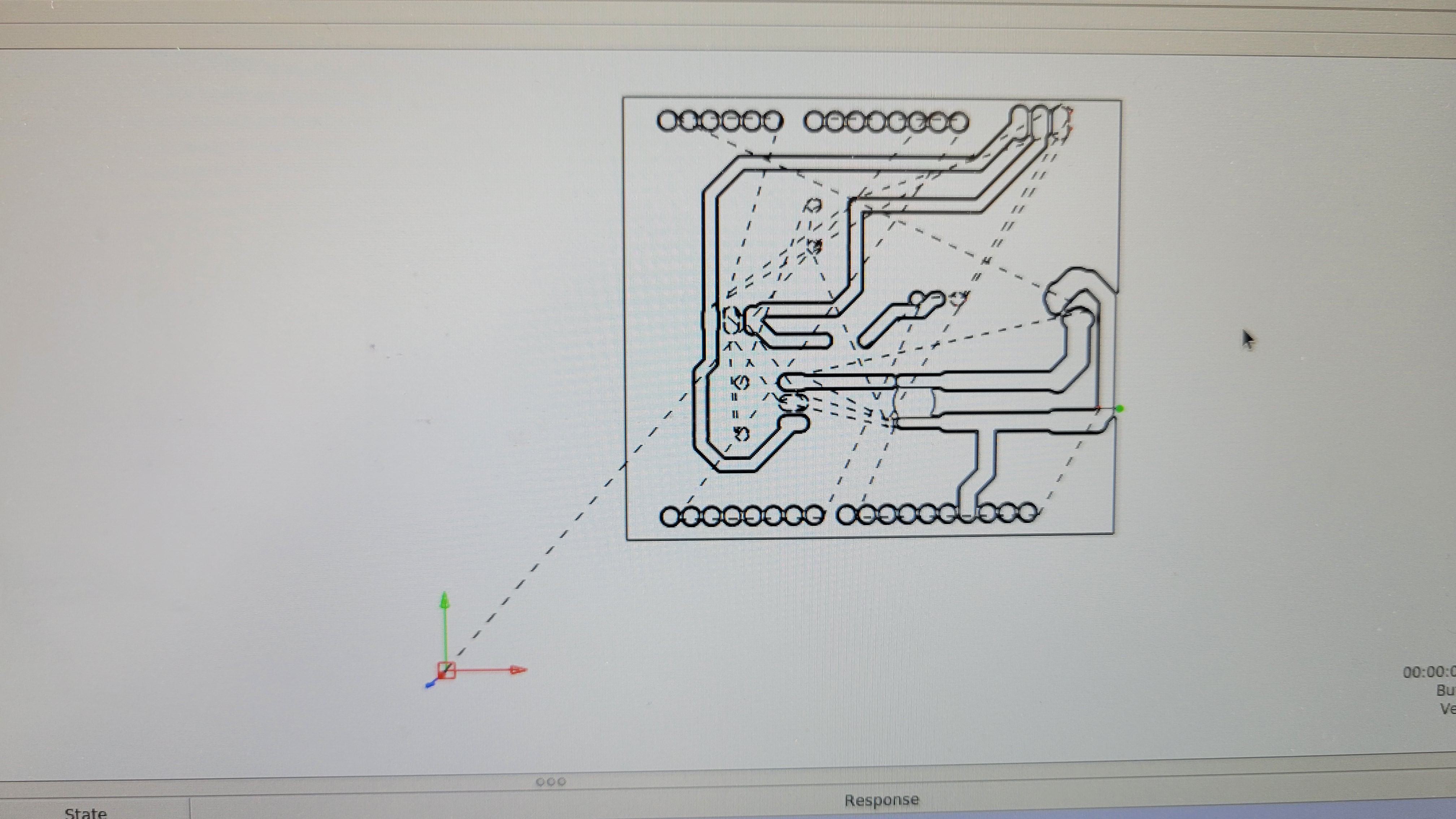
Converting it to GCode and sending to CNC/Candle software
Fingers crossed
[Hour later... and lots of noise]
After two hours of soldering I got this:
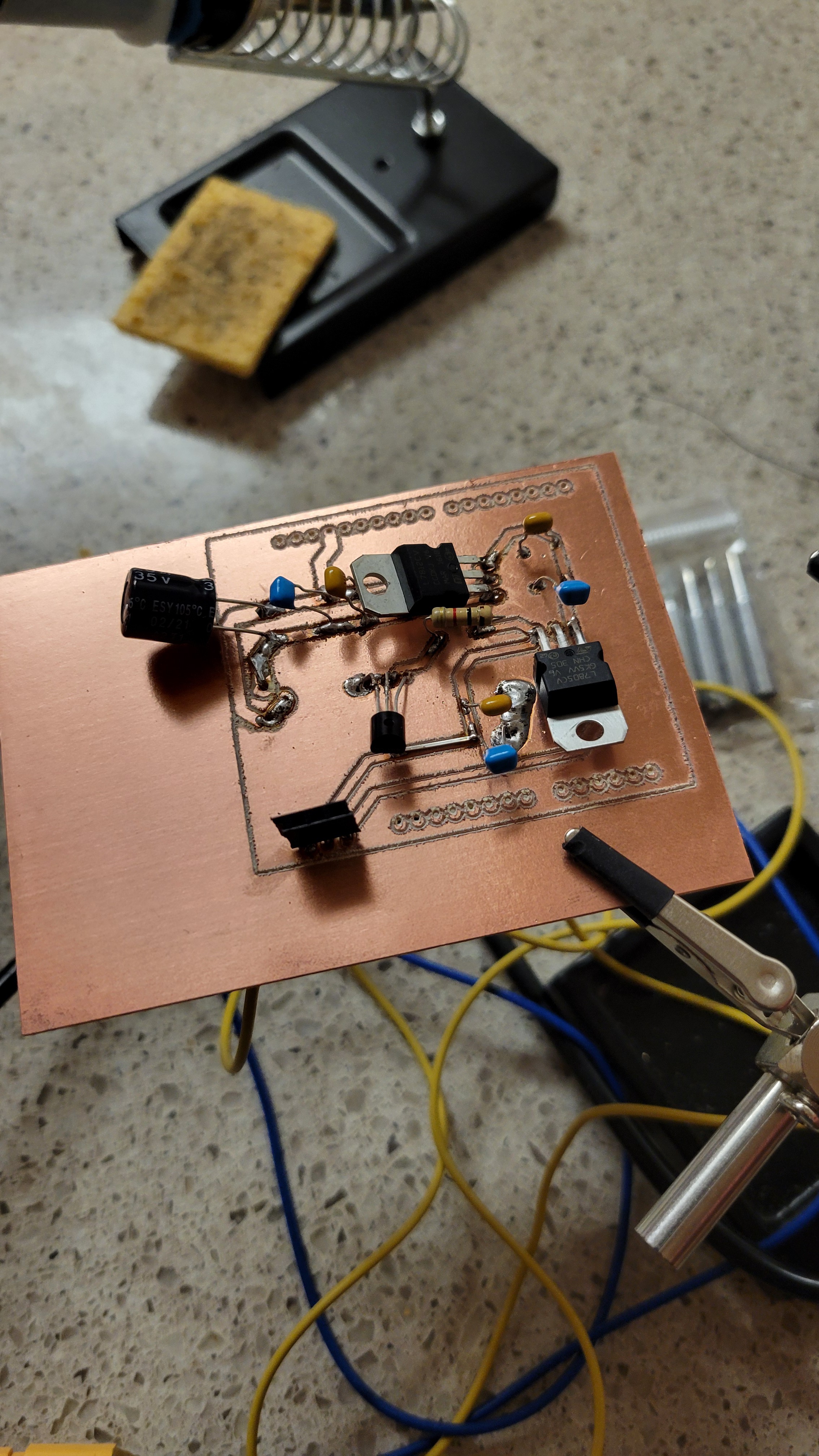
It's bit ugly but does what it suppose to do.
5v and 11v. Wait what? Why 11? It should be 12v.
One thing I've learned is to use wider pads for soldering otherwise connectors just breaks.
Single to double rail, here I come...
Anyway, the input should be 14.5v to 27v.
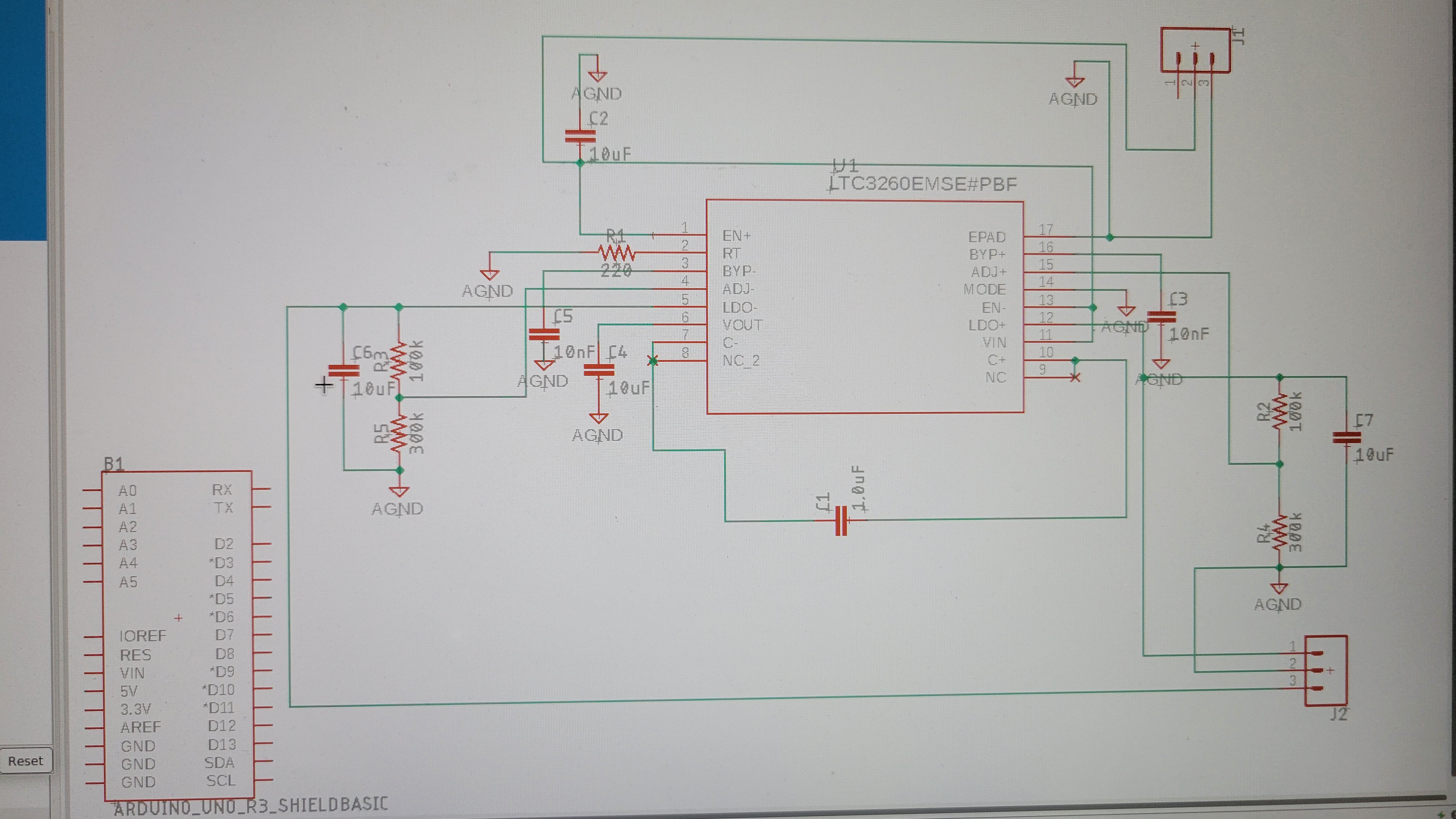
Now let's start with input. We should get -5 to +5 voltage for OPA656N to work.
Here is the schematic for generating two rails from one, using LT3260. Most of the time took me to learn how to import LT3260 into The result
The routing/placement will by difficult
---++++----
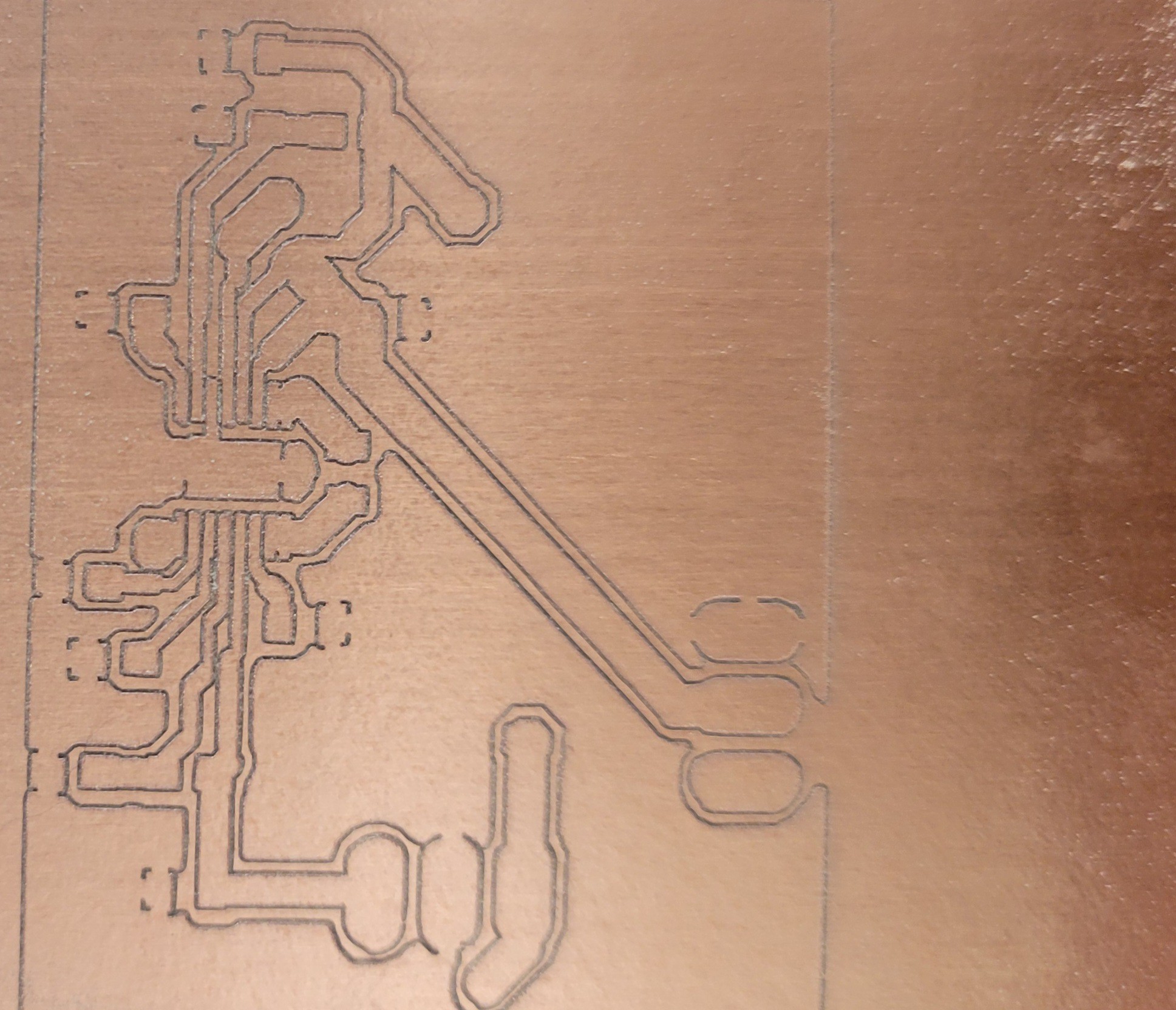
Actually it wasn't that difficult. I've used the one provided with LTC3260. I got this,
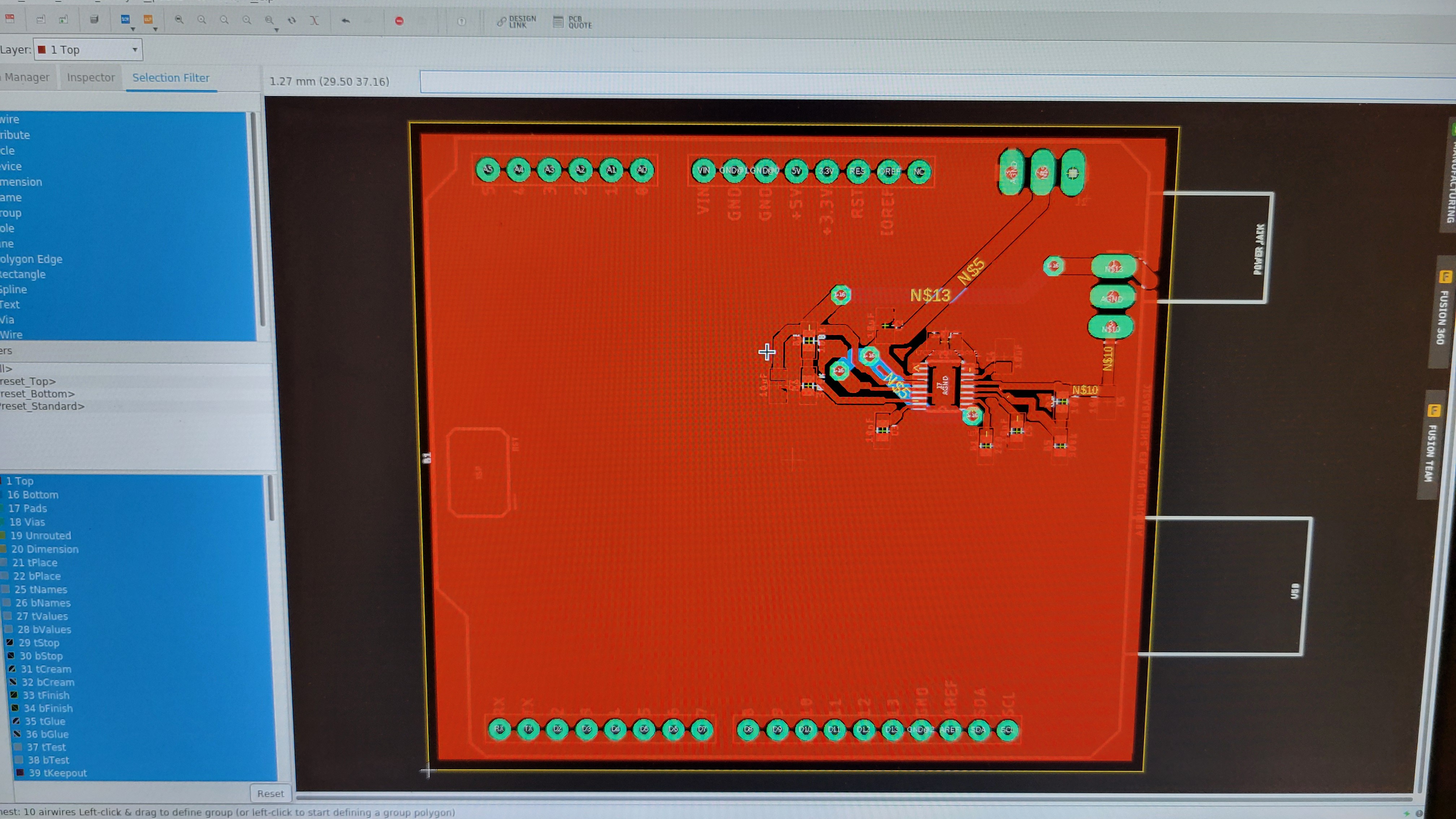
Let's zoom in..
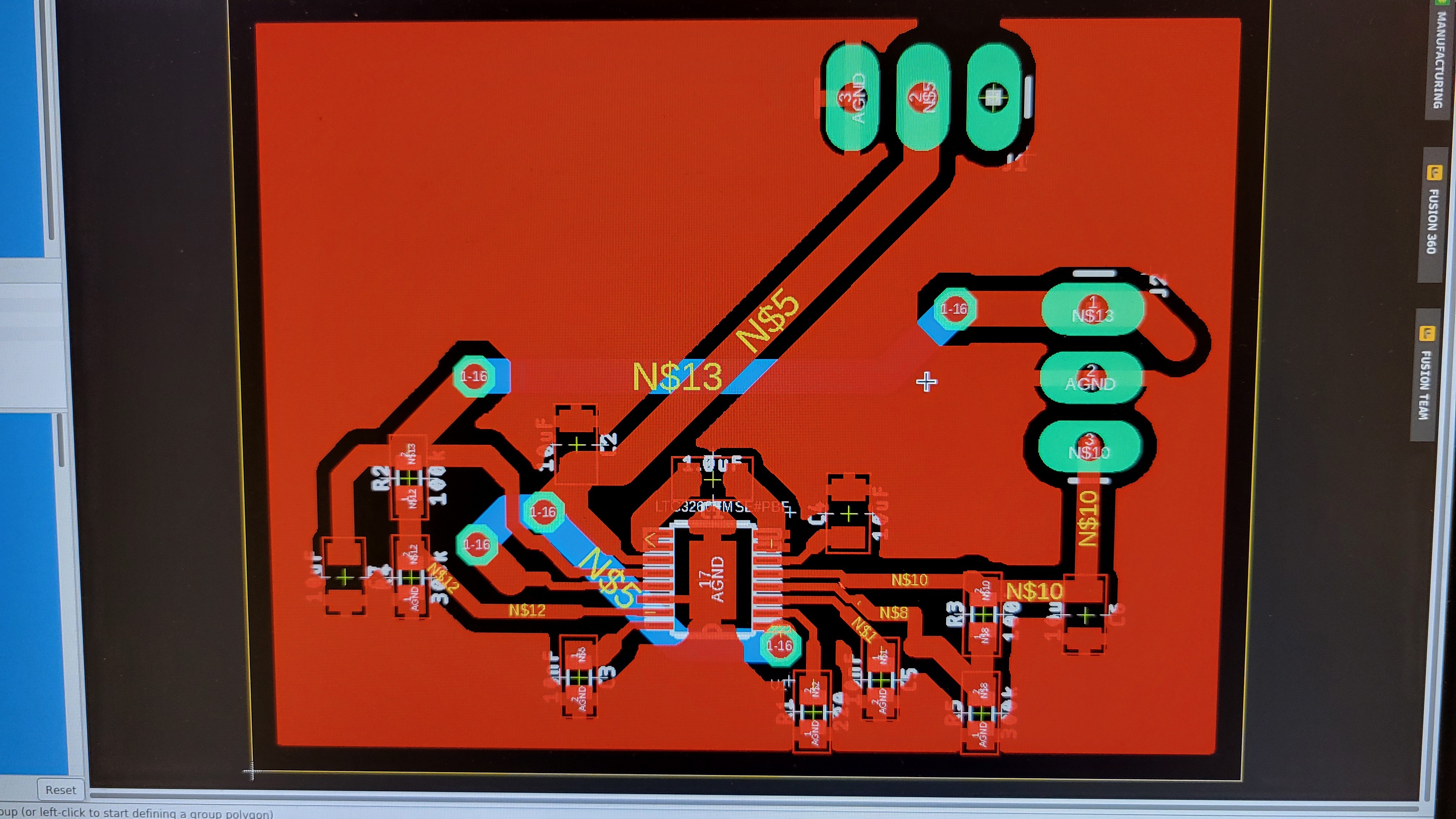
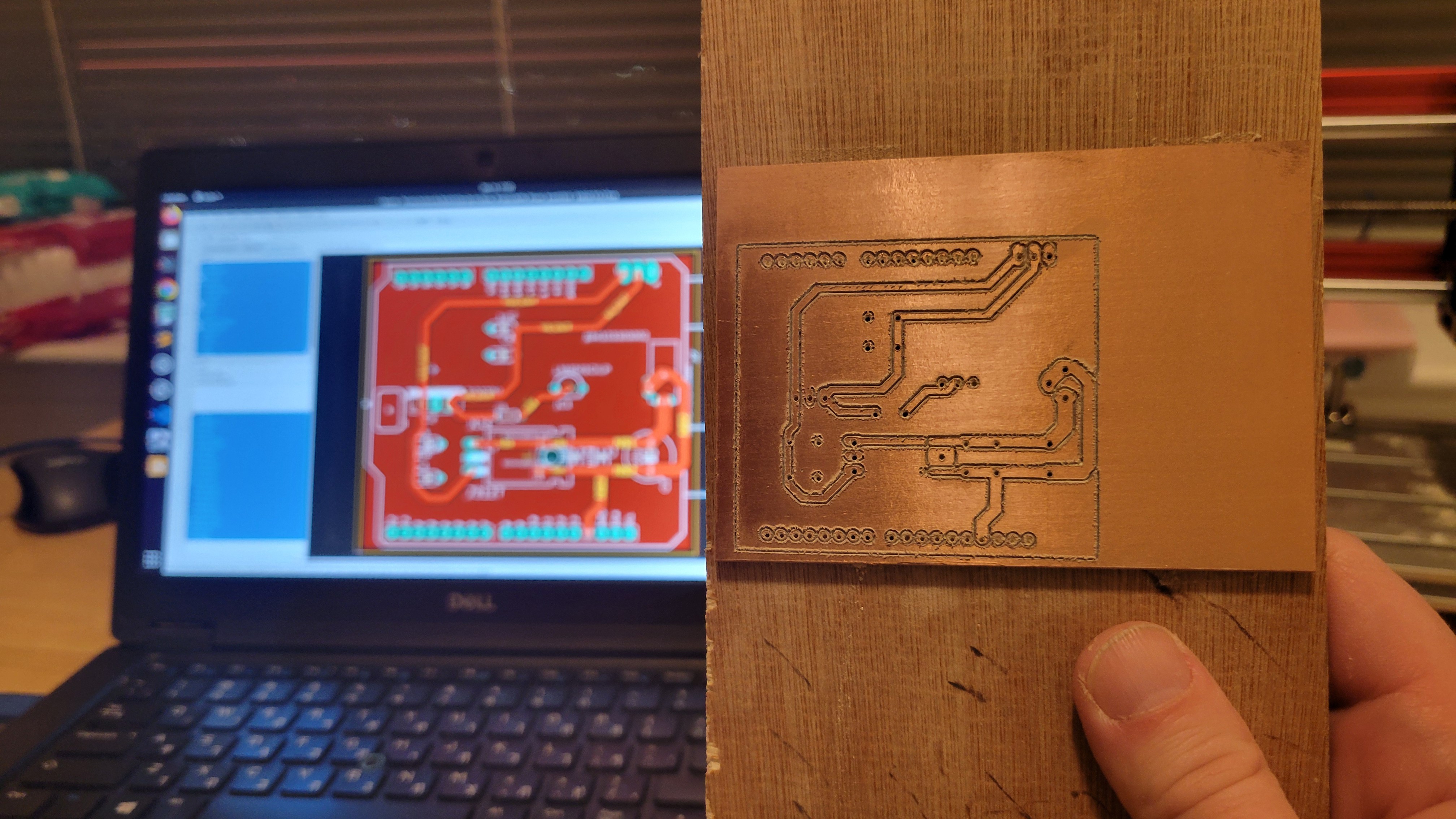
Now it's time to print and test it.
I know this is suboptimal, the vias are huge and I don't use smaller than 0603 capacitors/resistors.
And this all because I create PCBs manually, no dual copper layer etc.
On the other hand, I can change those designs in matter of hours 🙂
First looked good by after some examination it turns out to be bad, on GCode level.
The second one got broken bit in the middle. And third got wrong height for some reason.
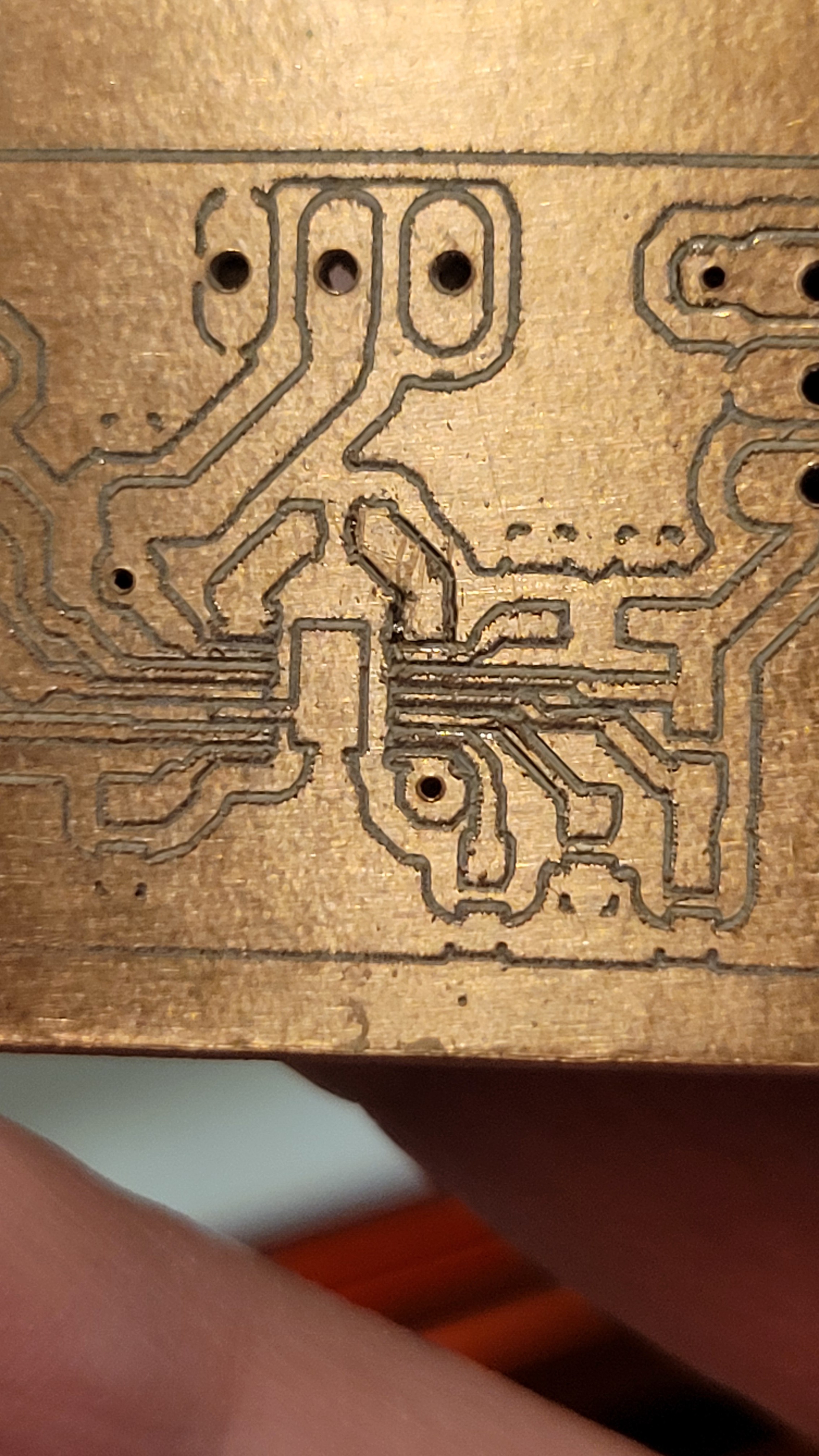
But fourth was much better,
More than I could ask from old and cheap CNC machine.
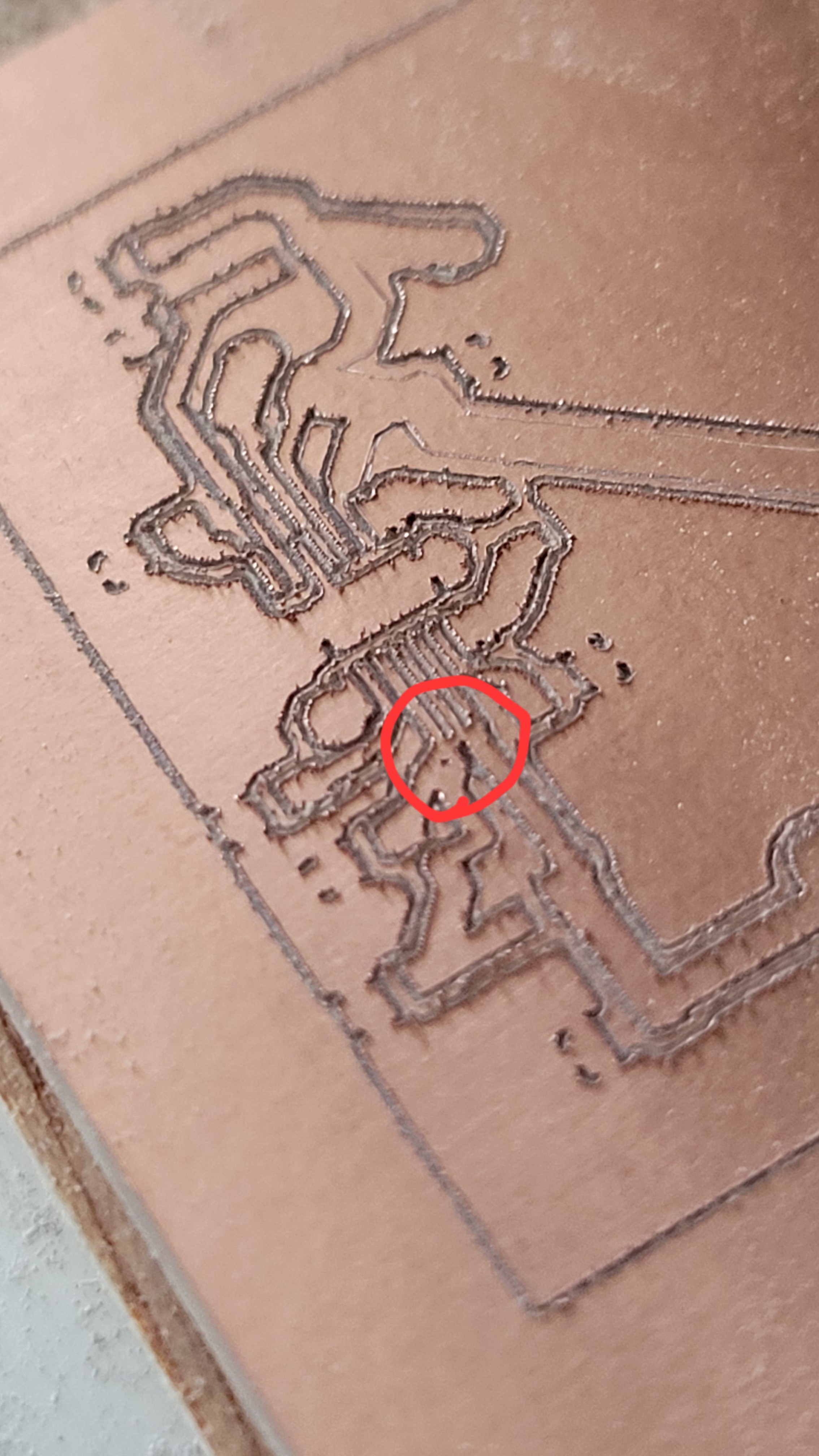
Checked the circuit for conductivity, one of the pads was short circuiting. Tried to fix it and bricked the PCB. Arrrr ...
Another three attempts ended up with two broken bits and one successful print. Made smaller circuit so printing would be faster.
It looks worse than the previous one but electricity wise it is ok.
Added all the components, boys it only looks easy.
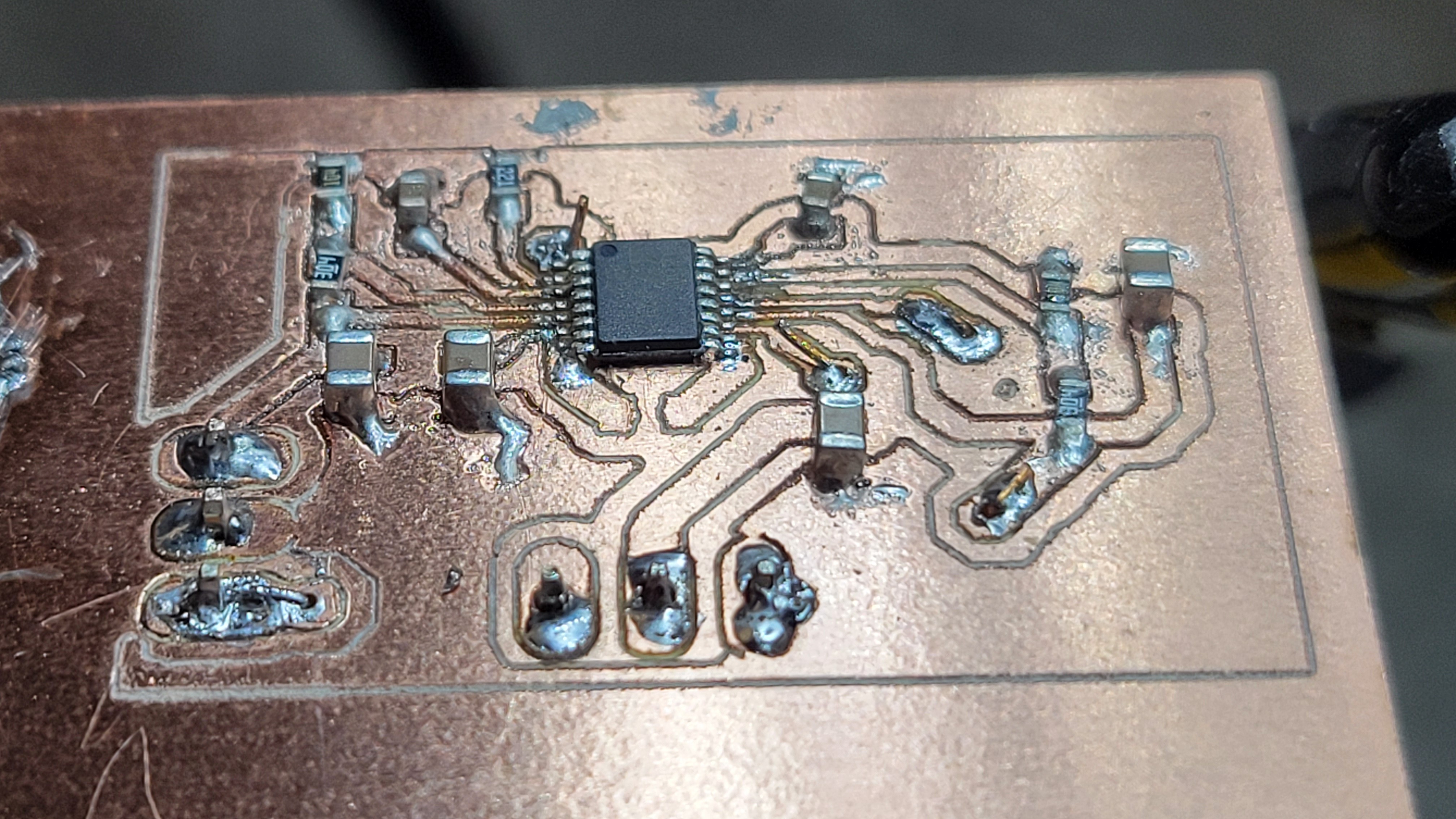
Soldering paste made things easier but components so tiny, it's crazy!
Checked all the lines, looks ok, except one. I hope I could fix it without bricking the PCB again.
The good news it's working!!
It's looks like I've made all possible mistakes one could think of.
First I managed to rotate power supply pins. Luckily I don't need Arduino inputs. Then from all capacitors I forgot charge pump capacitor.
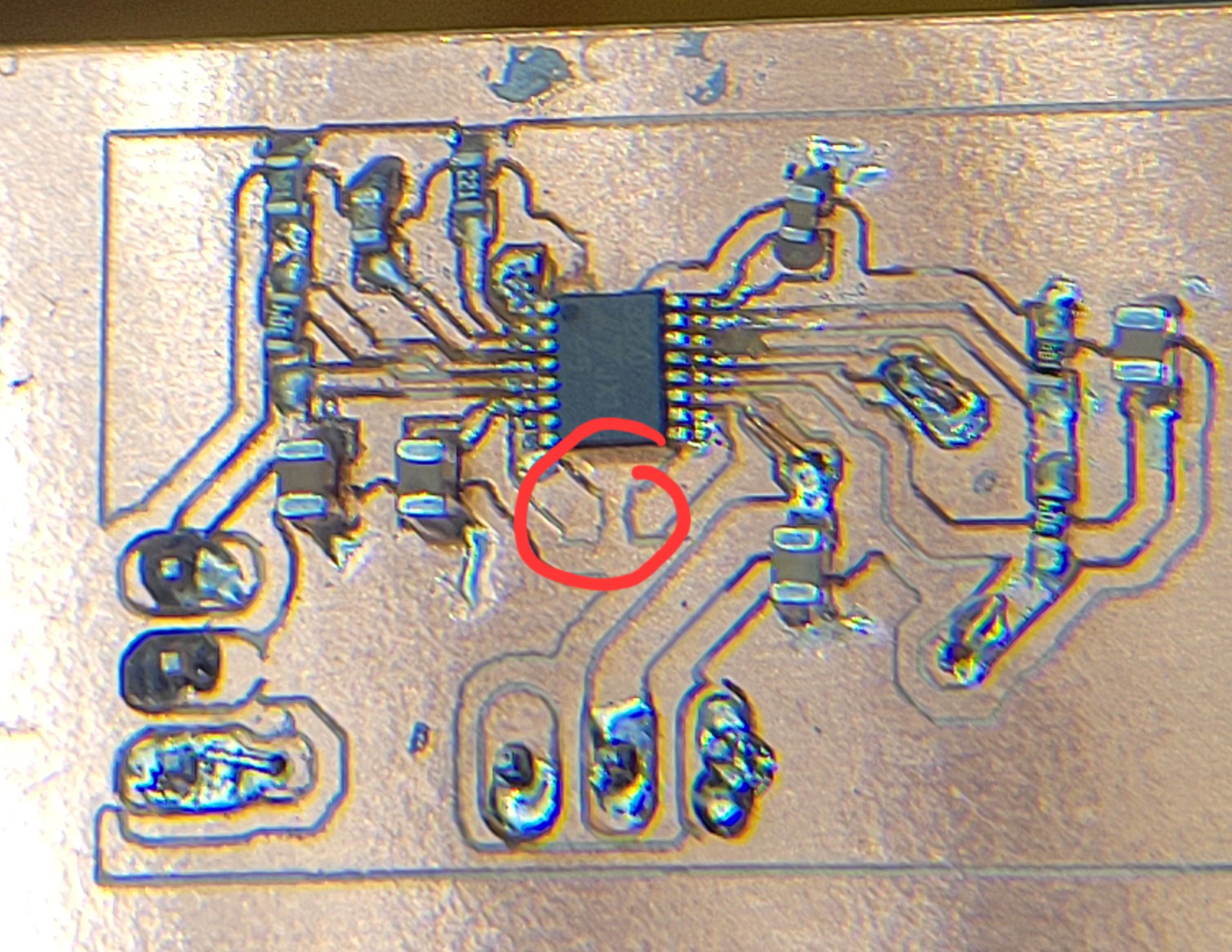
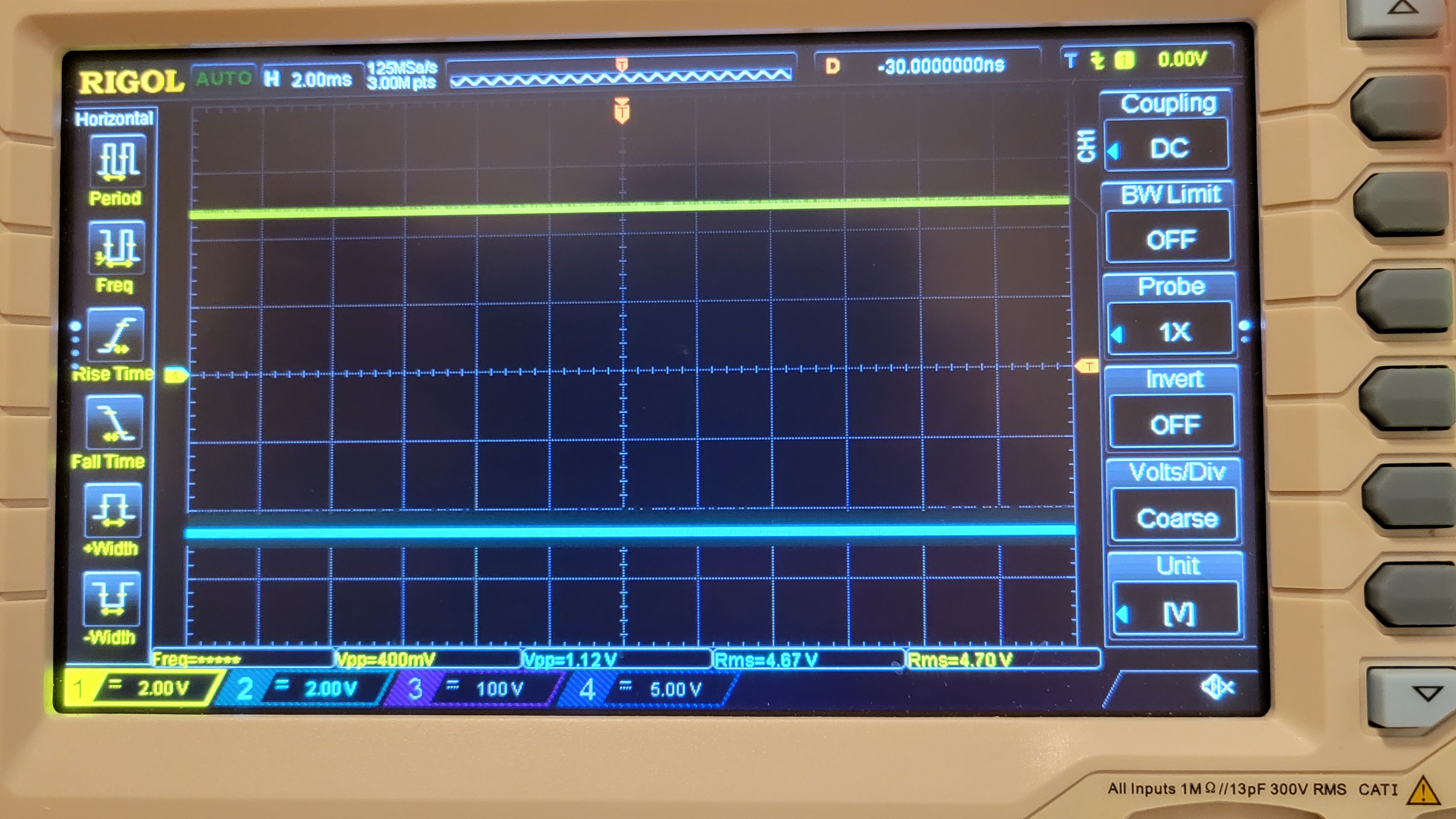
After connecting those it still didn't work. I thought first that I burned the IC by connecting wrong polarity. Luckily I got -5v Vo (not LDO-) so it encouraged me to look for a bug. Then I found that the problematic line was not problem with IC pins but near capacitors. Finally another problem was pin that was not properly connected, so when I checked it with Fluck it looked connected, but actually it was floating. Resoldering the pins gave finally the long waited results
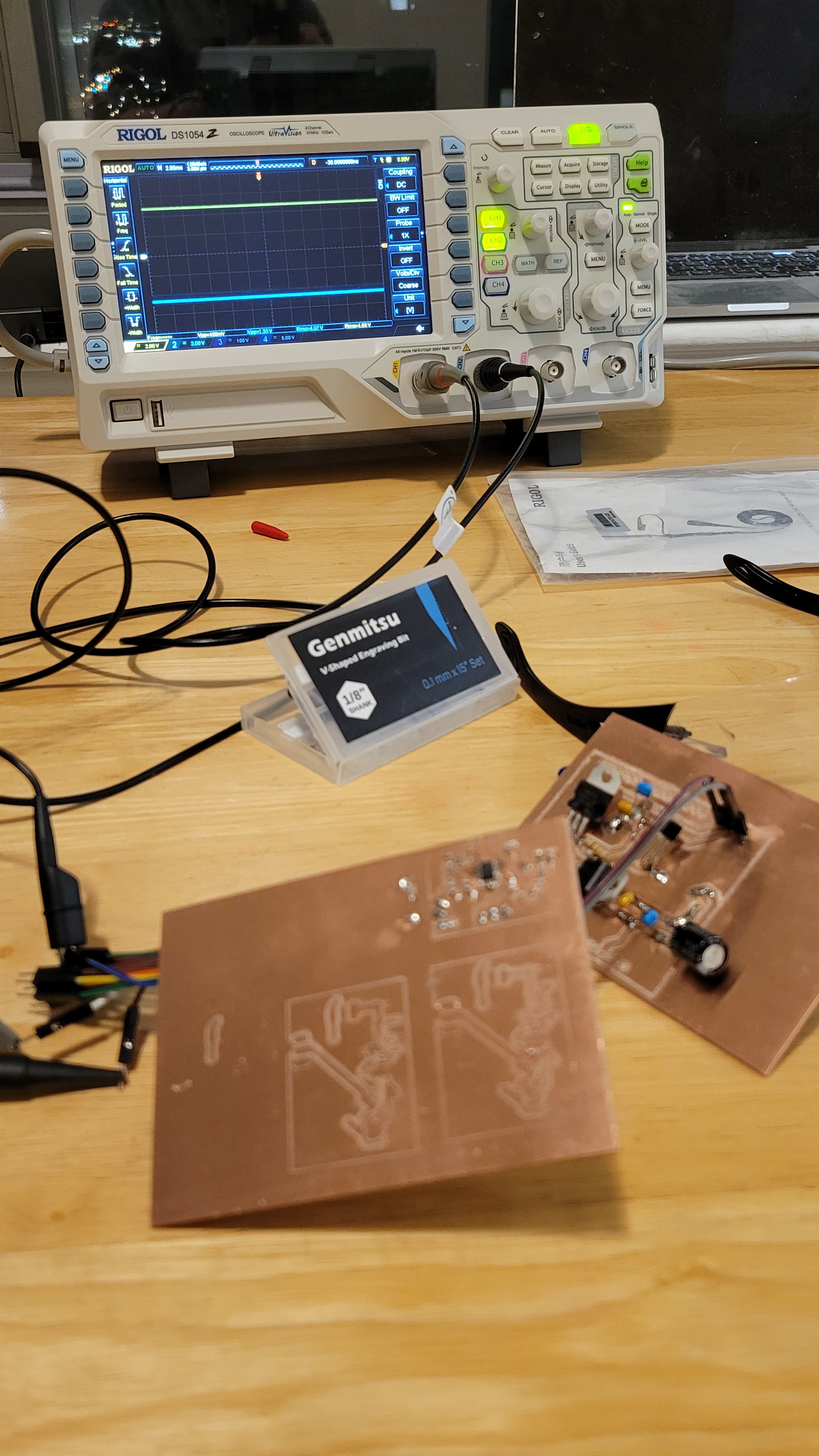
With stable output voltage
Discussions
Become a Hackaday.io Member
Create an account to leave a comment. Already have an account? Log In.