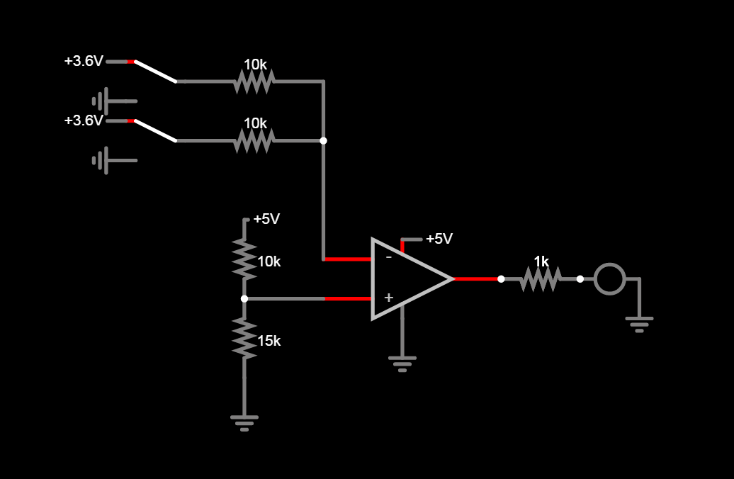
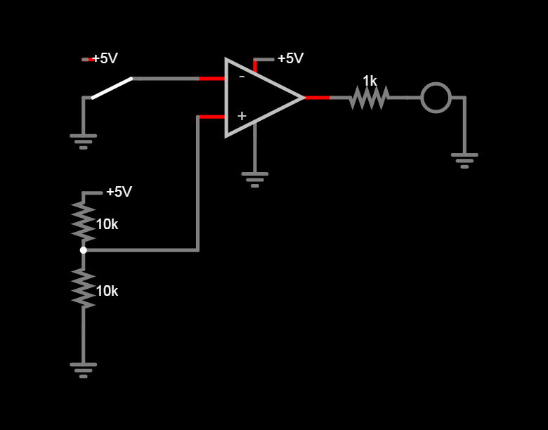
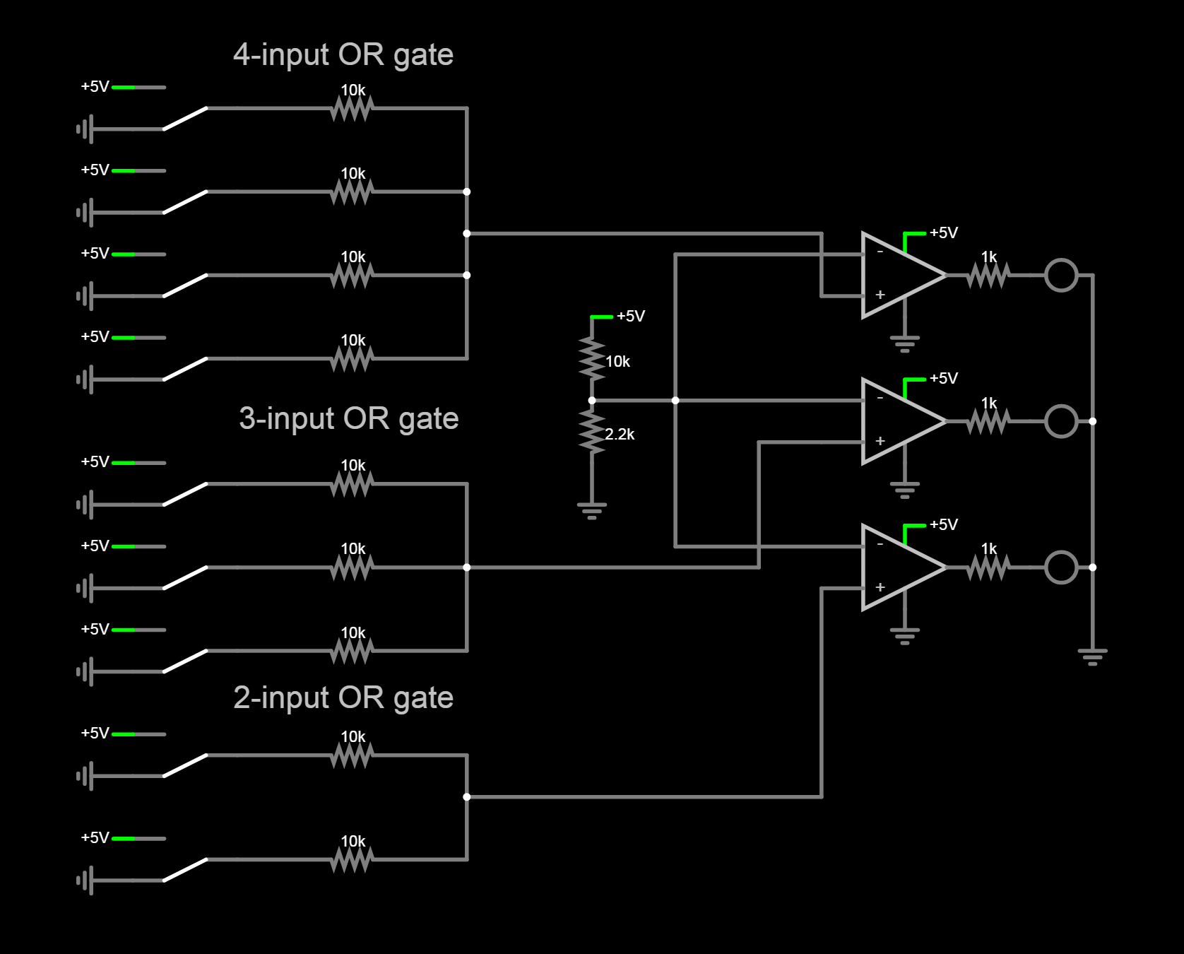
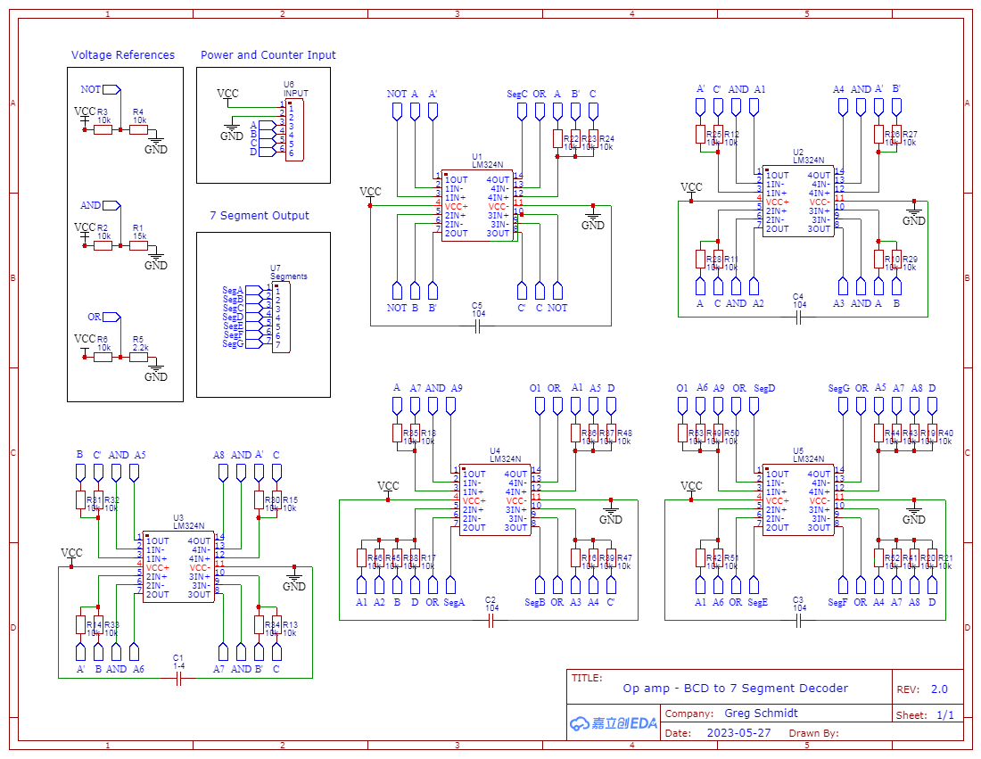
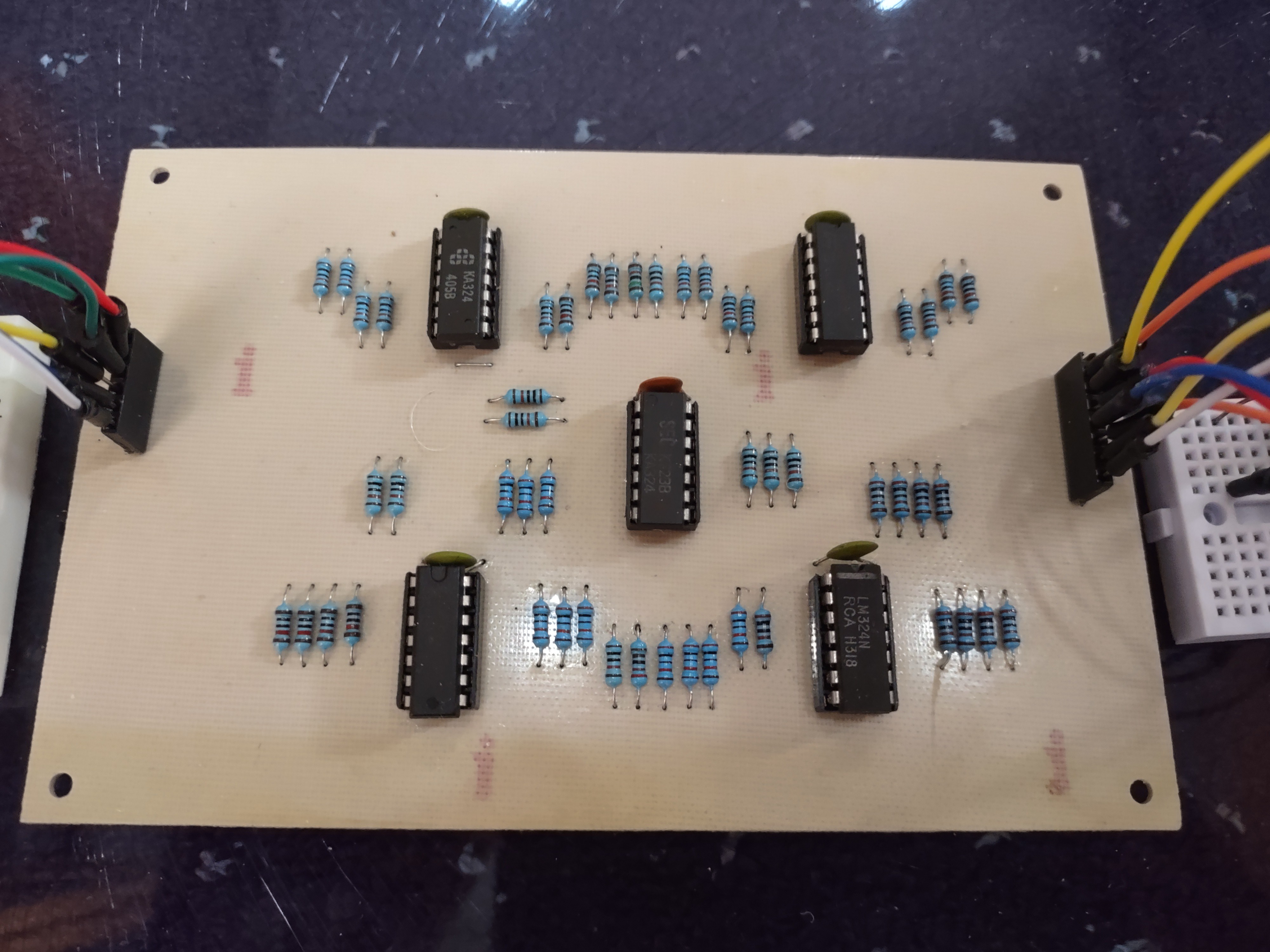
To simulate logic gates, the op amps are configured as open loop (no feedback) and effectively act as comparators. Each op amp "gate" is provided with an approriate Vref input via a resistor divider which causes it to swing to the high or low rail depending upon the value of the other input signal. The input signal consists of a resistor network which averages the voltage all of its input and provides that to the op amp input. The Vref voltages must be carefully chosen so as to ensure proper operation of the "gate". For example, the "OR" gate must trigger on a low threshold when any one of its inputs is high, conversely an "AND" gate have a higher threshold so that the op amp does not trigger when one input is present, but only when both inputs are high.
Further complicating the Vref determination is the fact that an LM324 can only reach approximately 3.6v (when powered by 5v), and so the gates must work properly with both 5v and 3.6v input voltages. The reason for that is due to the fact that the input to some gates are wired directly to the 5v inputs whereas the input to other gates are wired to the output of another gate that produces 3.6v. Yet another complication was the desire to use a single Vref for the variations of "OR" gates such that it works for the 2,3, and 4 input cases. Since all inputs are averaged, when only a single input is high, the average value will be lower for the 4 input "OR" gate than the 2 input "OR" gate.
The gate designs shown below were initially tested with the "Falstad" simulator. and then further tested on a breadboard.
I have uploaded Falstad code for the simulations shown below in the "Files" section of this project.
LM324 NAND gate. Since a digital computer can be constructed from NAND gates, it should be possible to build one using op amps as the basic building block. Therefore, op amps are capable of performing universal computation.
LM324 NOT gate (inverter)
LM324 AND gate:
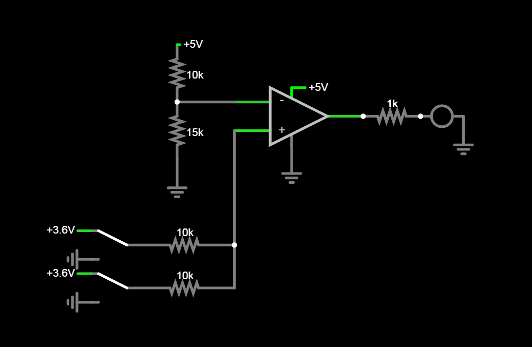
LM324 OR gates:
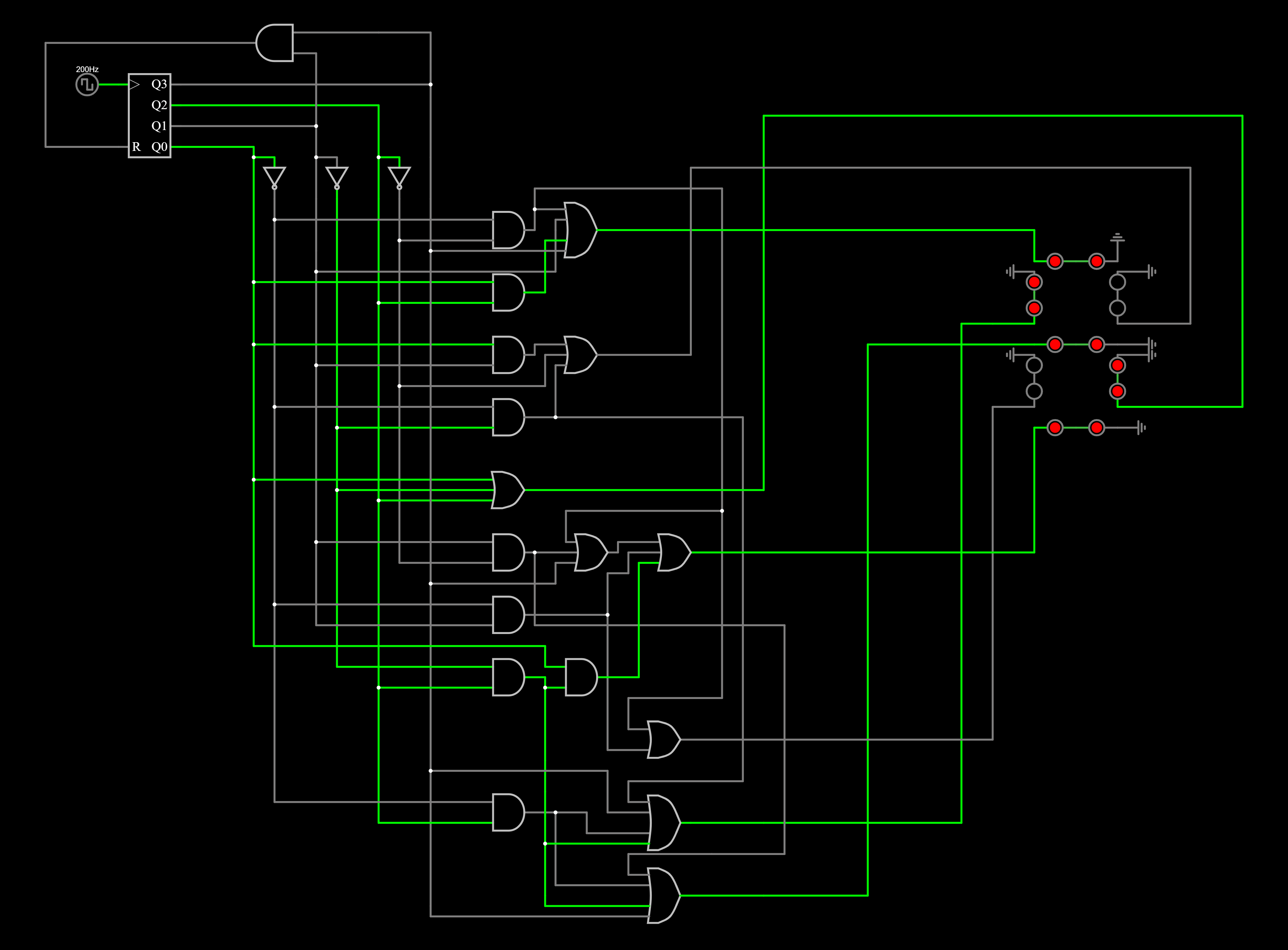
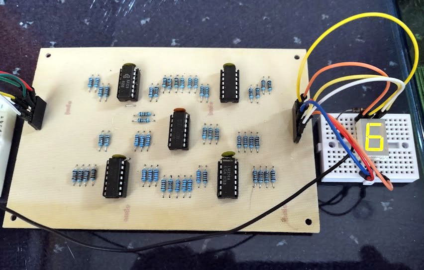
The logic design of the BCD to 7 segment converter:


 Tim
Tim
Great project, Bob Widlar would be proud. I wrote this up for the blog, should publish soon.
Thanks for participating in the contest. Good luck!